Switching power supply has an important position in the field of electronic power technology because of its advantages of low power consumption, high efficiency and light weight. The switching regulator power supply is mainly composed of a pulse width modulation (PWM) control chip, a MOSFET/IGBT and a transformer, and the time ratio of the on/off of the switching tube is controlled by the PWM to stabilize the power supply voltage output. As a power chip widely used in China, UC3842 has the advantages of fewer pins and simple peripheral circuits. In this paper, the protection circuit, the feedback circuit and the peripheral circuit of the switch tube are designed according to the characteristics of the chip. At the same time, the problems that should be paid attention to in the PCB layout and related suggestions are put forward. Finally, the feasibility of the multi-output of the circuit is verified by experiments.
1, UC3842 internal structure and application circuit diagramFigure 1 shows the internal block diagram of the UC3842. The 1 pin is the internal error amplifier output port. This pin forms a feedback network with the 2 pins, which makes the error amplifier compensation produce a stable closed-loop converter response and a large gain bandwidth. The 2 pin is the feedback voltage input terminal, and the feedback voltage is generated by the voltage input of the voltage divider resistor. The inverting terminal of the error amplifier is compared with the reference voltage divided by 2.5V to generate a voltage difference and thereby control the duty ratio of the output signal of the chip. The 3-pin is the current detection terminal, which converts the bus current into a voltage through a sampling resistor. When the voltage is greater than 1V, the PWM output of the chip is turned off, thereby protecting the circuit. The 4-pin is the internal oscillator input. The external Rt and Ct determine the operating frequency of the circuit. The 5 pin is the ground. The 6-pin is the output of the chip, and the output current is ±1A, which can directly drive the MOSFET. The 7-pin is the power supply terminal and is powered by the busbar through a voltage divider resistor. The 8-pin is the reference voltage output, providing an accurate 5V to the outside with a load capacity of 50mA.
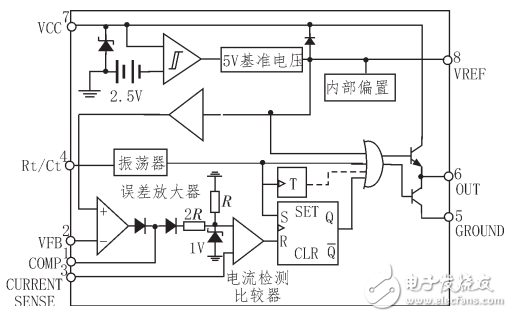
Figure 1 UC3842 internal structure
2. Analysis of the working principle of the application circuit1) AC-DC circuit
The AC-DC circuit turns the AC into a DC, which is a prerequisite for the design of a flyback switching power supply. Figure 2 shows an AC-DC circuit in which the input AC voltage is 60~220V, and the resistor 1R2 is a positive temperature coefficient thermistor to prevent overcurrent. 1R1 is a varistor used to bypass the surge voltage. In the PCB layout requirements, a serpentine trace is used between the varistor and the neutral line. If the varistor is damaged, the varistor can be disconnected in time without burning the circuit board because of the varistor short circuit. The common mode choke coil and the differential mode inductor (1L1, 1L2) respectively filter the common mode and differential mode interference, and the DC power is rectified by the full bridge rectifier bridge to supply power to the subsequent circuit.
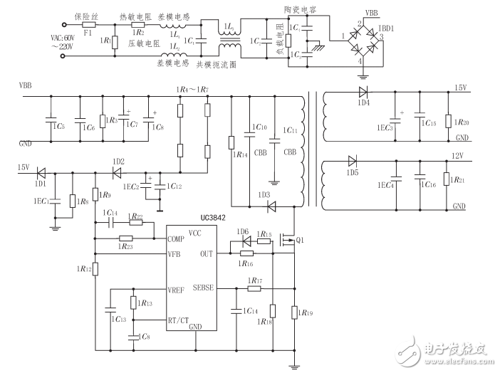
Figure 2 UC3842 application circuit schematic
Idc Connectors,Idc Socket Connector,Idc Electronic Socket Connector,2.00Mm Socket Connector
Dongguan Yangyue Metal Technology Co., Ltd , https://www.yyconnector.com