UHF RFID system air interface standards include ISO/IEC series, F2C series, and national standards being developed in China. Digital receivers can implement software upgrades and multi-protocol support. Compared with analog receivers, they are easy to debug and flexible. Advantages, and thus widely used in UHF 姗 readers. Improving the reading performance of UHF RFID readers has been the focus of research in recent years. After thorough analysis and experimental verification, this paper gives solutions to related problems.
UHF RFID readers use the backscatter principle to communicate with the tags. According to the current main UHF band air interface standard ISO/IEC 18000-6C, the tags communicate in the same frequency half-duplex mode in the passive state. . The basic communication process is that the reader modulates the carrier by means of amplitude shift keying (ASK), and transmits the information to one or more tags on a channel of a specific frequency. Afterwards, the reader still needs to transmit the CW carrier and wait for the response of the tag within the specified time.
The zero-IF architecture has the advantages of eliminating the need for an intermediate frequency link, reducing power consumption, reducing circuit complexity, and ease of debugging. The block diagram of the zero-IF RFID digital receiver is shown in Figure 1. The RF signal received by the antenna passes through the circulator and directly enters the down converter. The converted baseband signal is amplified by the LNA and low-pass filtered, and the two I and Q baseband signals are output to the baseband for digital signal processing.

Figure 1 Block diagram of zero IF RFID digital receiver
The communication effect of the reader is affected by parameters such as transmitter output power, receiver sensitivity, transmit/receive antenna gain, transceiver isolation, tag power consumption, tag antenna gain, and environmental conditions. Among them, the maximum effective omnidirectional transmit power (EIRP) of the transmitting end is regulated by the national radio transmitting equipment, and the transmission and reception isolation is limited by the isolation of devices such as the circulator (generally only 25dB), and the parameters in the tag, antenna and environment are certain conditions. The performance of the receiver plays a decisive role in the overall performance of the reader.
2 Analysis of factors affecting receiver performanceUHF RFID reader receivers also require the transmitter to transmit unmodulated carriers. The receiver receives signals including tag reflection, antenna noise, environmental reflection, direct coupling of the transmitter, and noise of the receiver itself. Under the premise that the tag can obtain enough working energy, the working distance of the reader mainly depends on whether the demodulated output of the tag backscattering signal can meet the minimum signal-to-noise ratio requirement. According to the literature [3], the following formula can be used to indicate the maximum working distance determined by the reader:

Where C is the propagation velocity of electromagnetic waves in free space, ω is the angular frequency of the electromagnetic wave signal, Г is the reflection coefficient of the tag power, ξ is the transmission and isolation isolation coefficient, GR is the antenna gain of the reader, Gt is the gain of the tag antenna, and the denominator Ppn represents the phase noise power in the single-sideband passband of the local oscillator. It can calculate the phase noise data known to the local oscillator or directly measure it using a spectrum analyzer (SPA). The PDATA in the numerator indicates the signal power in the single-side bandpass band of the binary data sequence of the tag, which can be obtained by numerical calculation. According to the formula, the working distance of the reader depends on the signal-to-noise ratio performance (SNR) of the receiver, especially the phase noise and the noise reduction processing effect, when the parameters such as the tag parameters, the antenna gain, and the transmission and reception isolation are constant.
The environment's catadioptric interference and phase noise are mainly near the carrier frequency. After down-conversion, it is characterized by low-frequency noise. The baseband signal is mixed with common high-frequency noise. In the dense reader mode, the receiver bandwidth needs to be controlled to avoid a certain range. The readers interfere with each other, so the baseband signal needs to be band-pass filtered to improve its signal-to-noise ratio.
The DC offset is a type of interference unique to the zero-IF architecture because the signal such as local oscillator, transmitter leakage, and environmental reflection in the receiver is coupled to the input of the mixer. The DC offset of the reader and receiver causes the DC offset to be much larger than that of the conventional receiver. The common working distance is only 3-5 meters. The carrier leakage is also affected by the antenna and the environment. The DC offset is time-varying. The DC offset not only destroys the DC operating point of the latter circuit, but also affects the linearity performance of the amplification filter circuit, which makes the signal-to-noise ratio worse. In a single-antenna design using a circulator, the circulator isolation is limited, resulting in high transmission leakage to the receiving end. The DC offset problem is more serious. DC offset, amplitude phase interference caused by environmental bounce, local oscillator phase noise, and ADC. Quantization noise, etc. can reduce the signal-to-noise ratio of the receiver, and improve its performance. In addition to improving on the analog RF circuit, it is necessary to take corresponding measures on the baseband signal processing algorithm.
3 baseband digital signal processingIn order to ensure the correct completion of the decoding, the baseband digital signal processing needs to complete the elimination of noise and interference, and complete the ASK signal decision in an appropriate manner. Key processing measures include oversampling and filtering, DC offset correction, and data decoding.
3.1 Oversampling and filtering
According to the Nyquist sampling theorem, in order to restore the sampled signal to the original continuous signal, the sampling frequency should be at least twice the highest frequency of the signal. Oversampling is based on the Nyquist frequency. The level of sampling doubling, oversampling can reduce the power of quantization noise in the effective bandwidth, improve the signal-to-noise ratio, which is equivalent to increasing the resolution of the ADC. The oversampled data can be extracted by the CIC filter, so that the data rate is returned. At normal levels, the cascaded FIR filter performs bandpass filtering to further reduce noise power and improve signal-to-noise ratio.
Taking the common ASK tag return signal with a code rate of 250 kbps as an example, in order to match the performance of the ADC chip, if the oversampling coefficient is selected to be 40, the sampling rate is 20 MSI 焉. The code rate after decimation is set to 8 times the code rate of the postback, that is, 2 Mbps, and the CIC filter level is 3.
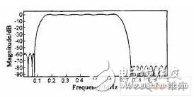
Most of the signal power of FM0 code is within the first zero point. Usually, the first zero point bandwidth position is twice the communication rate. After the clock jitter is added, the maximum first zero point bandwidth can reach 2.5 times the communication rate. Therefore, the low-pass cutoff frequency is set to 650 kHz; considering the V feature point of the sync head, the high-pass cutoff frequency can be set to 160 kHz to filter out-of-band noise as much as possible under limited resource conditions. Figure 2 is a plot of the amplitude-frequency characteristic of the designed bandpass filter.

Fig. 2 The amplitude-frequency characteristic curve of the bandpass filter
3.2 DC offset correction
Methods for processing DC offset by circuit hardware include: AC coupling, carrier cancellation, harmonic mixing, self-correction compensation, etc. Among them, harmonic mixing processing and self-correcting compensation methods are complicated, and the effect of implementation is limited. . Reference [4] refers to a processing method for carrier cancellation, which requires simultaneous addition of compensation circuits and software in analog RF and baseband units, which increases complexity and cost, and is difficult to debug. Reference [5] mentions that the DC part of the signal can be filtered out by capacitive AC coupling to reduce the interference of DC offset. This method is the simplest and lowest cost of all schemes, and thus the most widely used.
The data frame synchronization header of the label retransmission includes a number of preamble zero plus preambles, and the baseband program can start decoding and receiving information after detecting the synchronization header within a prescribed time. Although the AC coupling method can alleviate the interference caused by signal overload, since the reader operates in the burst communication mode, the step response characteristic of the receiving circuit will cause a ramp effect at the sync head position, which often leads to synchronization error determination. The median correction can be performed before the baseband signal processing. The method only needs to perform sliding window tracking and pp value averaging on the collected data. The principle is:

In the above formula, c is the value of the calibrated ADC data, i is the data number, x(i) is the original data value, Y(i) is the correction result data of the point, n is the size of the sliding window, and j is the sliding window calculation. Serial number.
In addition to the fact that part of the data header cannot be recovered due to distortion, the synchronization header data of the communication frame can be restored with a small computational cost, thereby reducing the influence of DC offset interference on decoding synchronization.
3.3 Data decoding
The baseband data decoding method is divided into two types: zero-crossing detection and coherent detection. The zero-crossing detection works by setting a threshold, and comparing each data sample in the data buffer with the median value, if the data sample is in the middle If the absolute value of the difference of the values ​​is greater than the threshold and greater than the average value, it is judged as 1, otherwise it is judged as 0. Because the method is simple and easy to implement, even the comparator can be used to realize the judgment, which is widely used in low-end and mid-range reader products.
Coherent detection has better decoding ability, and can achieve far better performance than zero-crossing detection in the environment where the input signal is relatively poor. Because FM0 coding adopts orthogonal coding, it satisfies:

Before decoding, the data arrays S0 and S1 need to be created in advance as symbol templates for 0 and 1 representing FMO encoding. According to the formula, the input data is correlated with S0 and S1, respectively, and the result of the operation represents the degree of correlation between the input signal and the symbol 0 and the symbol 1. The symbol template sets the segment length according to the sampling multiple, and the correlation operation is also segmented in the same manner. Since the symbol templates S0 and S1 are also orthogonal, which operation result value is larger, it indicates which symbol the representative data represents. Since the tag return signal allows a frequency offset of ±22%, the starting position of the segment coherent calculation is difficult to define. The design of reference [6] uses a method of simultaneous calculation into multiple sets of correlators, which occupies more FPGA resources. A better way is to use zero-crossing detection comprehensively, and correct the starting position of the segment at intervals of 3-4 cycles, thus ensuring that the segmentation calculation process is always synchronized with the signal cycle, so that the resource consumption is not excessively increased. The same effect can still be achieved.
4 verification and analysisAccording to the above analysis, the prototype verification platform is designed. The digital signal processing of the baseband is completed by Altera Cyclone II FPGA. The functions implemented include ADC driver, FIFO buffer, CIC filtering and correlation judgment. The processing of the protocol flow is assigned to the soft core embedded in the FPGA. After the CPU completes, the above function block is attached to the internal bus of the soft core CPU in the manner of a peripheral device. The design of all function blocks is based on the standard IP library provided by Altera. The transmitter antenna port output power is 30dBm, the working frequency is 915MHz, and the 7dBi circularly polarized antenna is used. The label uses Alien products. Set the tag 8m away from the antenna and control the tag's return rate to 250kdBs.
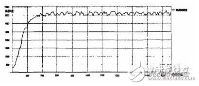
The raw data curve acquired by the ADC is shown in Figure 3 (the horizontal axis is the number of samples and the vertical axis is the sample data value). Since the complete communication frame data is large, only the first half of the I path data including the synchronization header and the synchronization code and the processing result thereof are given here.

Figure 3 Raw data curve acquired by ADC
It can be seen that in the zero-IF receiving analog output, in addition to the required tag return data, the data frame sync header is also mixed with DC offset interference and high-frequency noise. Due to the long distance, the useful signal has a pp value of only 110, the waveform distortion is severe, and the signal-to-noise ratio is relatively poor.
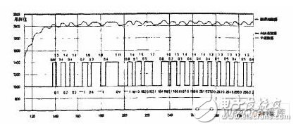
After CIC and bandpass filtering, the curve shown in Fig. 4 can be obtained. At this time, the filter removes the mixed noise, and the waveform becomes relatively smooth and tidy, and the synchronization header and data bits of the data frame can be easily distinguished. The figure also shows the decoding curve of zero-crossing detection (located below the graph, the square wave is marked with 0 and 1 of the zero-crossing detection and the number of sample points; the decoding result is marked below. 2B4: 0, indicating the second byte The 4th bit is decoded to 0), and the algorithm has a decoding decision error (1B5:1, symbol 0 is judged as 1) on the left side of the horizontal axis coordinate 240, indicating that the distortion handling capability is limited.

Figure 4 Direct zero-crossing detection decoding effect
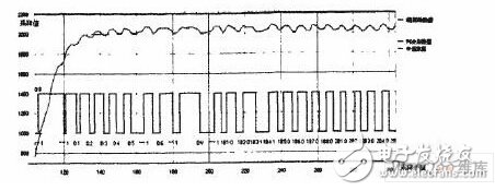
At the same time, the same data is processed by DC offset correction and coherent detection method. The curve and effect obtained are shown in Fig. 5. The decoding result waveform display algorithm improves the decoding effect of the sync header. At the same time, the left side of the horizontal axis coordinate 240 is correctly decoded (1B5:0), which proves that the algorithm can still obtain the EPC data correctly if the amplitude of the return signal of the long-distance tag is relatively small or the median value of the tag signal fluctuates.

Figure 5 DC offset correction and coherent detection decoding effect
5 ConclusionThis paper analyzes the performance bottleneck in the design of zero-IF architecture UHF RFID reader digital receiver, and clarifies the causes and solutions of noise interference, DC offset and decoding problems that affect the receiving performance. From the perspective of baseband digital signal processing, based on the oversampling filtering process, solutions such as DC offset correction and correlation decoding are given. After testing and verification, the reader can stably read the label with a distance of about 10m, and can adapt to the changes of the antenna and the environment. The reading effect is more stable and reliable than the common products on the market. It proves that the design requirements for increasing the working distance of the reader are achieved.
Original compatible with usable medical device battery, authorized by authentic manufacturer
On time delivery, factory inspection, 5 years warranty
Defibrillator Battery
Shenzhen Sunwind Energy Tech Co.,Ltd , https://www.sunwindbatterylm.com