PCB layout
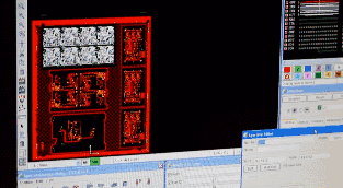
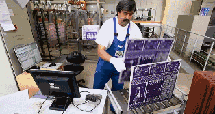
The first step in PCB fabrication is to organize and inspect the PCB layout. The PCB production factory receives the CAD files from the PCB design company. Since each CAD software has its own unique file format, the PCB factory will be converted into a unified format - Extended Gerber RS-274X or Gerber X2. Then the factory engineer will check whether the PCB layout conforms to the manufacturing process and whether there are any defects.
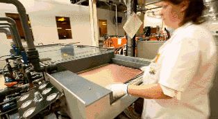
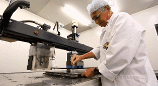
In the first phase of home-made PCB information, the PCB layout was printed on paper with a laser printer and then transferred to a copper clad laminate. However, in the printing process, since the printer is prone to ink breakpoints, it is necessary to manually fill the ink with an oil-based pen.
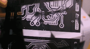
A small amount of production is OK, but if this defect is transplanted to industrial production, it will greatly reduce production efficiency. Therefore, the factory generally uses a photocopying method to print the PCB layout on the film. In the case of a multi-layer PCB, each layer of photocopied layout film will be arranged in order.
The film will then be aligned. It is important to align the holes, and then to align the material of each layer of the PCB, it depends on the alignment holes.
Core board production
Cleaning the copper clad plate may cause a short circuit or open circuit in the final circuit if there is dust.
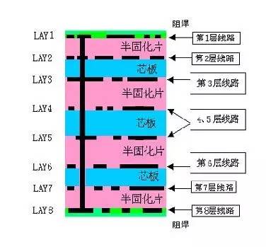
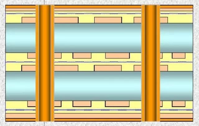
The figure below is an illustration of an 8-layer PCB. It is actually made up of 3 copper clad plates (core plates) plus 2 copper films, which are then bonded together with prepregs. The production sequence starts from the middlemost core board (4, 5 layer lines), is constantly stacked together, and then fixed. The production of the 4-layer PCB is similar, except that only one core board and two copper films are used.
Inner PCB layout transfer
So first make the two layers of the most core core (Core). After the copper clad plate is cleaned, a photosensitive film is placed on the surface. The film will cure when exposed to light, forming a protective film on the copper foil of the copper clad laminate.
The two-layer PCB layout film and the double-layer copper-clad board are finally inserted into the upper-layer PCB layout film to ensure accurate stacking position of the upper and lower PCB layout films.
The photosensitive machine irradiates the photosensitive film on the copper foil with a UV lamp, and the photosensitive film is cured under the light-transmissive film, and the photosensitive film is not cured under the opaque film. The copper foil covered under the cured photosensitive film is the required PCB layout circuit, which is equivalent to the function of the laser printer ink of the manual PCB. In the paper PCB layout of the previous laser printer, the black toner under the cover was the copper foil to be retained. In this period, the copper foil covered by the black film will be etched away, and the transparent film is retained because the photosensitive film is cured.
The uncured photosensitive film is then washed away with lye, and the desired copper foil line will be covered by the cured photosensitive film.
Inner core plate etching
The unwanted copper foil is then etched away with a strong base such as NaOH.
The cured photosensitive film is torn off to expose the required PCB layout copper foil.
Core plate punching and inspection
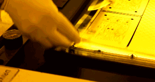
The core board has been successfully produced. Then, the alignment holes are made on the core board to facilitate alignment with other materials.
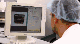
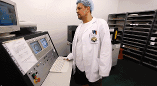
Once the core board is pressed together with the other layers of the PCB, it cannot be modified, so the inspection is very important. The machine will automatically compare with the PCB layout drawing to see the error.
The first two layers of PCB board have been completed.
laminated
A new material called Prepreg is needed here, which is the core and core board (>2 layers of PCB), and the adhesive between the core board and the outer layer of copper foil, and also acts as insulation.
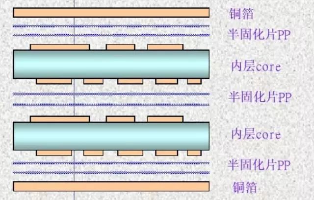
The lower layer of copper foil and the two layers of prepreg have been fixed in advance through the alignment hole and the lower iron plate, and then the prepared core plate is also placed in the alignment hole, and finally two layers of prepreg, a layer of copper foil and A layer of pressure-bearing aluminum plate covers the core.
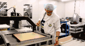
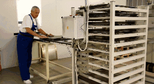
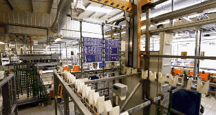
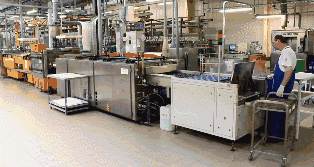
In order to improve work efficiency, the factory will stack 3 different PCB boards and fix them. The upper iron plate is magnetically attracted to facilitate alignment with the lower iron plate. After the two layers of iron plates are successfully aligned by inserting the alignment pins, the machine compresses the space between the iron plates as much as possible, and then fixes them with nails.
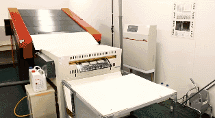
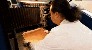
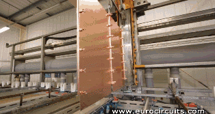
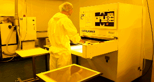
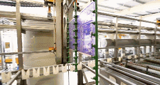
The PCB boards sandwiched by the iron plates are placed on the holders and then fed into a vacuum hot press for lamination. The high temperature in the vacuum hot press melts the epoxy in the prepreg and holds the core and copper foil under pressure.
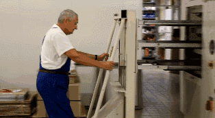
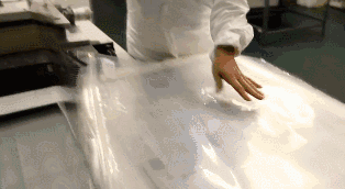
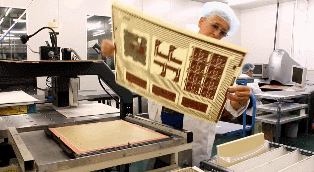
After the lamination is completed, the upper iron plate of the pressed PCB is removed. The pressure-bearing aluminum plate is then removed, and the aluminum plate also serves to isolate the different PCBs and ensure the smoothness of the outer copper foil of the PCB. Both sides of the PCB taken out at this time will be covered by a layer of smooth copper foil.
drilling
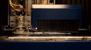
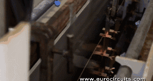
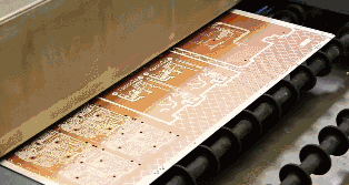
So how do you connect the four layers of copper foil that are not in contact with each other in the PCB? First, the perforation through the top and bottom is drilled to open the PCB, and then the hole wall is metalized to conduct electricity.
The X-ray drilling machine is used to position the core layer of the inner layer. The machine will automatically find and locate the hole on the core board, and then position the PCB with a positioning hole to ensure that the next hole is drilled from the center of the hole. Over.
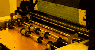
Place a layer of aluminum on the puncher machine and place the PCB on top. Since drilling is a relatively slow process, in order to improve efficiency, one to three identical PCB boards are stacked together for perforation according to the number of layers of the PCB. Finally, the uppermost PCB is covered with an aluminum plate. The upper and lower layers of the aluminum plate are used to not tear the copper foil on the PCB when the drill bit is drilled and drilled.
The operator then only needs to select the correct drilling program and the rest is done automatically by the drill. The drill bit is driven by air pressure and has a maximum rotation of 150,000 rpm. This high speed is enough to ensure the smoothness of the hole wall.
The replacement of the drill bit is also done automatically by the machine according to the program. The smallest drill bit can reach a diameter of 100 microns, while the diameter of a human hair is 150 microns.
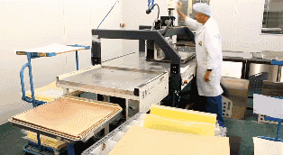
In the previous lamination process, the melted epoxy was extruded outside the PCB, so removal was required. The mold milling machine cuts the periphery of the PCB according to the correct XY coordinates of the PCB.
Copper chemical precipitation of pore walls
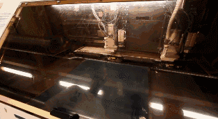
Since almost all PCB designs are lines of different layers that are connected by perforations, a good connection requires a 25 micron copper film on the walls of the holes. This thickness of copper film needs to be achieved by electroplating, but the walls of the holes are composed of non-conductive epoxy and fiberglass sheets. So the first step is to first deposit a layer of conductive material on the wall of the hole, and form a 1 micron copper film on the entire surface of the PCB, including the hole wall, by chemical deposition. The entire process, such as chemical processing and cleaning, is controlled by the machine.
Fixed PCB
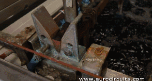
Cleaning the PCB
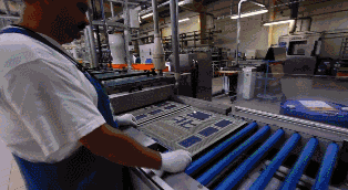
Shipping PCB
Chemical precipitation copper film
Outer PCB layout transfer
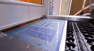
Next, the outer PCB layout will be transferred to the copper foil. The process is similar to the previous inner core PCB layout transfer principle. The photocopying film and photosensitive film are used to transfer the PCB layout to the copper foil, the only difference. It will be a positive film.
The transfer of the inner PCB layout introduced earlier is based on the subtractive method, which uses a negative film. The circuit covered by the cured photosensitive film on the PCB is used to clean away the unsolidified photosensitive film, and after the exposed copper foil is etched, the PCB layout line is protected by the cured photosensitive film. The transfer of the outer PCB layout is based on the normal method, using a positive film. The cured film on the PCB is covered by a non-line area. Electroplating is performed after cleaning the uncured photosensitive film. There is no film at the film, and there is no film, first plated with copper and then tin plated. After the film is removed, alkaline etching is performed, and finally the tin is removed. The line pattern remains on the board because it is protected by tin.
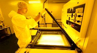
The PCB with the double-sided copper foil is placed in a laminating machine, and the laminating machine presses the photosensitive mold onto the copper foil.
The PCB layout film of the upper and lower layers is fixed by the positioning hole, and the PCB board is placed in the middle. The photosensitive film under the light-transmissive film is then cured by irradiation of a UV lamp, that is, a line that needs to be retained.
After cleaning off the unwanted, non-cured photosensitive film, it is inspected.
Clamp the PCB with a clip and plate the copper. As mentioned before, in order to ensure that the hole position has sufficient conductivity, the copper film plated on the hole wall must have a thickness of 25 microns, so the whole system will be automatically controlled by the computer to ensure its accuracy.
Fixed PCB
Computer control and electroplating copper
After the copper plating is completed, the computer will also arrange a thin layer of tin.
After unloading the tin-plated PCB board, check to ensure that the thickness of the plated copper and tin is correct.
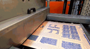
Outer PCB etching
The etching process is then completed by a complete automated pipeline. First, the cured film on the PCB is washed away.
The undesired copper foil covered by it is then washed away with a strong alkali.
Then remove the tin plating on the copper foil of the PCB layout with tin-removing liquid. After cleaning, the 4-layer PCB layout is complete.
Product categories of Cloth Pen Nib, it is belong to Passive Stylus Pen. Passive stylus pen is characterized by being cheap and without charging. But compared with the active capacitive stylus pen, its tip diameter is larger, so it cannot be used in works with high precision. Using high-quality conductive cloth head, smooth contact with the screen.
Cloth Pen Nib,Multi-Functional Pen Stylus Pen,Stylus Pencil With Clip,Touch Stylus Pencil
Shenzhen Ruidian Technology CO., Ltd , https://www.wisonen.com