IGBT (Insulated Gate Bipolar Transistor) is a composite fully-regulated voltage-driven power semiconductor device composed of BJT (Bipolar Transistor) and MOS (Insulated Gate Field Effect Transistor), which combines the high input impedance of MOSFET and The advantages of the GTR's low on-voltage drop. The GTR saturation voltage is reduced, the current carrying density is large, but the driving current is large; the MOSFET driving power is small, the switching speed is fast, but the conduction voltage drop is large, and the current carrying density is small.
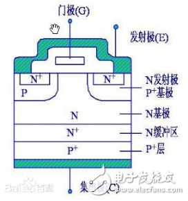
The figure below shows an N-channel reinforced insulated gate bipolar transistor structure. The N+ region is called the source region, and the electrode attached to it is called the source (ie, emitter E). The N base is called the drain area. The control region of the device is the gate region, and the electrode attached thereto is called the gate (ie, gate G). The channel is formed next to the boundary of the gate region. The P-type region (including the P+ and P-regions) between the C and E poles (the channel is formed in this region) is called a sub-channel region. The P+ region on the other side of the drain region is called the drain implant region. It is a functional region unique to the IGBT. Together with the drain region and the sub-channel region, a PNP bipolar transistor is formed, which acts as an emitter and injects empty into the drain. The hole is electrically modulated to reduce the on-state voltage of the device. The electrode attached to the drain implant region is referred to as the drain (ie, collector C).
The switching function of the IGBT is to form a channel by adding a forward gate voltage, and provide a base current to the PNP (formerly NPN) transistor to turn on the IGBT. Conversely, the reverse gate voltage is applied to eliminate the channel, and the base current is cut off to turn off the IGBT. The driving method of the IGBT is basically the same as that of the MOSFET, and it only needs to control the input pole N-channel MOSFET, so it has high input impedance characteristics. When the channel of the MOSFET is formed, the hole from the P+ base is injected into the N-layer (small sub-), and the N-layer is conductance modulated to reduce the resistance of the N-layer, so that the IGBT also has a low voltage at a high voltage. On-state voltage.
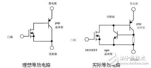
2, IGBT worksAs can be seen from the figure, if a positive driving voltage is applied between the gate and the emitter of the IGBT, the MOSFET is turned on, so that the collector and the base of the PNP transistor are in a low-resistance state, so that the transistor is turned on; When the voltage between the gate and the emitter is 0V, the MOSFET is turned off, and the supply of the base current of the PNP transistor is cut off, so that the transistor is turned off.
The ideal equivalent circuit and actual equivalent of IGBT are shown in the figure:
SHENZHEN CHONDEKUAI TECHNOLOGY CO.LTD , https://www.siheyidz.com