IC package picture Daquan

Noun interpretation

COF (Chip On Flex, or Chip On Film, often called flip chip)
The technology of fixing the IC to the flexible film structure of the flexible circuit board is a technique of bonding the chip and the flexible substrate circuit by using a soft additional circuit board as a package chip carrier.
COG(Chip on glass)
That is, the chip is directly bonded to the glass. This method can greatly reduce the size of the entire LCD module, and is easy to mass-produce, and is used in consumer electronic products such as mobile phones, PDAs, and the like.
DIP (dual in-line package)
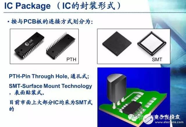
Dual in-line package. One of the plug-in packages, the leads are led out from both sides of the package, and the package materials are plastic and ceramic. DIP is the most popular plug-in package, and its application range includes standard logic IC, memory LSI, and microcomputer circuit. The pin center is 2.54mm apart and the number of pins is from 6 to 64. The package width is typically 15.2mm. Some packages with widths of 7.52mm and 10.16mm are called skinny DIP and slim DIP (narrow body DIP). However, in most cases, there is no distinction. They are simply referred to as DIP. In addition, ceramic DIP sealed with low melting point glass is also known as cerdip.
PDIP
P-Plasti, indicating the mark of the plastic package. For example, PDIP stands for plastic DIP.

SDIP (shrink dual in-line package)
Shrinkage type DIP. One of the cartridge type packages has the same shape as the DIP, but the pin center distance (1.778mm) is smaller than DIP (2.54mm), hence the name. The number of pins is from 14 to 90. Also known as SH-DIP. The materials are ceramic and plastic.
SKDIP/SKY (Skinny Dual In-line Packages)
A type of DIP. Refers to a narrow body DIP with a width of 7.62 mm and a center-to-center spacing of 2.54 mm. Often referred to collectively as DIP (see DIP).
DIP-tab
A type of DIP.
CDIP
C-ceramic, the mark of the ceramic package. For example, CDIP stands for ceramic DIP. It is a mark that is often used in practice.

DICP(dualtapecarrierpackage)
Double-sided pin-loaded package. One of TCP (loaded package). The leads are fabricated on the insulating tape and pulled out from both sides of the package. Due to the TAB (Automatic On-Load Soldering) technology, the package is very thin. It is commonly used in liquid crystal display driver LSIs, but most of them are fixed products. In addition, a 0.5 mm thick memory LSI booklet package is in the development stage. In Japan, DICP is named DTP according to the EIAJ (Japan Electromechanical Industry) standard.

DIC(dualin-lineceramicpackage)
Another name for ceramic DIP (including glass seal).
SIP (single in-line package)
Single in-line package. The leads are drawn from one side of the package and arranged in a straight line. The package is side-mounted when assembled onto a printed substrate. The lead center distance is usually 2.54mm and the number of pins is from 2 to 23, most of which are custom products. The shape of the package varies. Some packages that have the same shape as ZIP are called SIP.
SOP (Small Outline Packages)
Small outline pin package.

SSOP (Shrink Small-Outline Package)
In a narrow-pitch, small-profile plastic package, Philips developed a small outline package (SOP) from 1968 to 1969.
TSOP (Thin Small Outline Package)
It means a small, small package. The TSOP memory is pinned around the chip and is attached directly to the surface of the PCB using SMT technology (surface mount technology).
TSSOP (Thin Shrink Small Outline Package
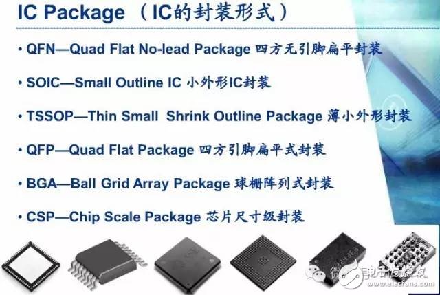
Thin reduced SOP. Thinner than SOP, the pins are denser, and the package size is smaller with the same function.
HSOP (Head Sink Small Outline Packages)
H-(with heat sink), indicating a mark with a heat sink. For example, HSOP stands for SOP with a heat sink.

DFP (dual flat package)
Double-sided pin flat package. It is another name for SOP (see SOP). I used to have this method before, but now I have basically not used it. 10. Another name for DIC (dual in-line ceramic package) ceramic DIP (including glass seal) (see DIP).
DSO(dual small out-lint)
Double-sided pin small outline package. Another name for SOP (see SOP). Some semiconductor manufacturers use this name.
MFP (mini flat package)
Small flat package. Another name for plastic SOP or SSOP (see SOP and SSOP). The name adopted by some semiconductor manufacturers.
SO(small out-line)
Another name for SOP. Many other semiconductor manufacturers in the world use this nickname. (see SOP).

SOIC(small out-line integrated circuit)
Another name for SOP (see SOP). Many semiconductor manufacturers abroad use this name.
SOJ (Small Out-Line J-Leaded Package)
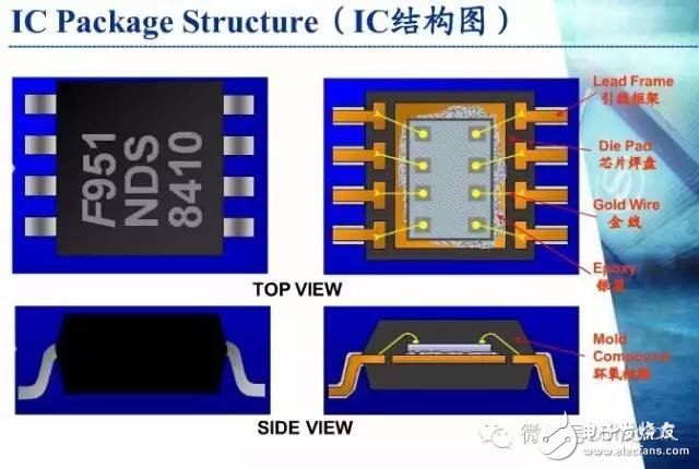
J-shaped pin small outline package. One of the surface mount packages. The pin is drawn from both sides of the package and is J-shaped downward, hence the name. Usually plastic products, mostly used in memory LSI circuits such as DRAM and SRAM, but most of them are DRAM. Many DRAM devices packaged in SOJ are mounted on SIMM. The center of the pin is 1.27mm and the number of pins is from 20 to 40 (see SIMM).
SOT (Small Outline Transistor)
Small external transistor, one of the SOP series packages.
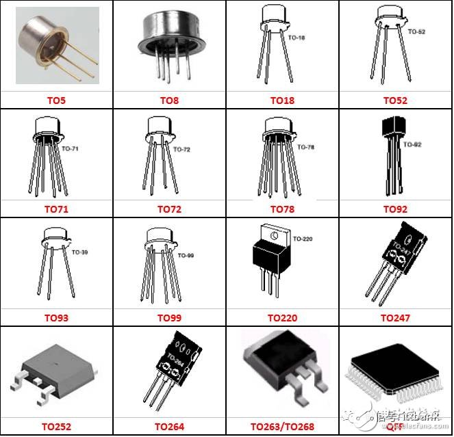
TO(Transistor Outline)
Transistor package.
QFP (quad flat package)
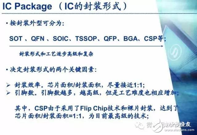
Four-sided pin flat package. One of the surface mount packages, the leads are drawn from four sides into a gullwing (L) type. The substrate is available in ceramic, metal and plastic. In terms of quantity, plastic packaging accounts for the vast majority. When no material is specifically indicated, it is mostly plastic QFP. Plastic QFP is the most popular multi-pin LSI package. It is used not only for digital logic LSI circuits such as microprocessors and gate displays, but also for analog LSI circuits such as VTR signal processing and acoustic signal processing. The center distance of the pins is 1.0mm, 0.8mm, 0.65mm, 0.5mm, 0.4mm, 0.3mm, etc. The maximum number of pins in the 0.65mm center-to-center specification is 304. In Japan, QFP with a pin center distance of less than 0.65 mm is called QFP (FP). But now the Japanese electromechanical industry has re-evaluated the QFP's form factor. There is no difference in the center distance of the pins, but it is divided into QFP (2.0mm ~ 3.6mm thick), LQFP (1.4mm thick) and TQFP (1.0mm thick) according to the thickness of the package body . In addition, some LSI manufacturers refer to QFPs with a 0.5mm lead pitch as shrink-type QFP or SQFP or VQFP. However, some manufacturers also refer to the QFP with a pin center distance of 0.65mm and 0.4mm as SQFP, which makes the name slightly confused. The disadvantage of QFP is that the pins are easily bent when the center distance of the pins is less than 0.65 mm. In order to prevent pin deformation, several improved QFP varieties have emerged. BQFP with a tree-finger cushion at the four corners of the package (see BQFP); GQFP with a resin guard ring covering the front end of the pin (see GQFP); set test bumps in the package body and prevent pin deformation The TPQFP can be tested in a dedicated fixture (see TPQFP). In terms of logic LSI, many development products and high reliability products are packaged in the multilayer ceramic QFP. Products with a minimum center-to-center distance of 0.4mm and a maximum of 348 pins have also been introduced. In addition, glass-sealed ceramic QFPs are also available (see Gerqa d).

LQFP (low profile quad flat package)
Thin QFP. Refers to the QFP with a package body thickness of 1.4mm, which is the name used by the Japan Electromechanical Industry Association according to the new QFP form factor.
MQFP (metric quad flat package)
A classification of QFPs in accordance with JEDEC (United States Joint Electronic Equipment Council) standards. Refers to a standard QFP with a center-to-pin distance of 0.65mm and a body thickness of 3.8mm to 2.0mm (see QFP).
TQFP (Thin Quad FLat Packages)
Thin plastic package in a four-corner flat package.
SQFP (Shorten Quad FLat Packages)
Reduced pin pitch QFP.

BQFP(quad flat package with bumper)
Quad flat-lead package with pad. One of the QFP packages has protrusions (cushions) at the four corners of the package body to prevent bending deformation of the pins during shipping. US semiconductor manufacturers use this package primarily in circuits such as microprocessors and ASICs. The center of the pin is 0.635mm and the number of pins is from 84 to 196.
PQFP (PlasticQuadFlatPackage)
The plastic is led out of the flat package.
FQFP (fine pitch quad flat package)
The small pin center is from the QFP. Usually refers to a QFP with a pin pitch less than 0.65mm (see QFP). Some conductor manufacturers use this name.
PFPF (plastic flat package)
Plastic flat package. Another name for plastic QFP (see QFP). The name adopted by some LSI manufacturers.

QFN(quad flat non-leaded package)
Four-sided, leadless flat package. One of the surface mount packages. Now more called LCC. QFN is the name given by the Japan Electromechanical Industry Association. The four sides of the package are equipped with electrode contacts. Due to the absence of leads, the placement area is smaller than QFP and the height is lower than QFP. However, when stress is generated between the printed substrate and the package, no relief can be obtained at the electrode contact. Therefore, the electrode contacts are difficult to make as many pins as the QFP, generally from about 14 to about 100. The materials are ceramic and plastic. When there is an LCC mark, it is basically a ceramic QFN. The center of the electrode contacts is 1.27 mm. Plastic QFN is a low cost package of glass epoxy printed substrate. In addition to the 1.27mm center distance of the electrode contacts, there are two types of 0.65mm and 0.5mm. This package is also known as plastic LCC, PCLC, P-LCC, and the like.
LCC (Leadless chip carrier)
Leadless chip carrier. Refers to the surface mount package with no electrodes on the four sides of the ceramic substrate. It is a package for high speed and high frequency ICs, also known as ceramic QFN or QFN-C (see QFN).
PLCC (plastic leaded chip carrier)
Plastic chip carrier with leads. One of the surface mount packages. The pins are drawn from the four sides of the package and are T-shaped, which is a plastic product. Texas Instruments, Inc., first used in 64k-bit DRAM and 256k DRAM, is now widely used in circuits such as logic LSIs and DLDs (or logic devices). The center of the pin is 1.27mm and the number of pins is from 18 to 84. The J-shaped pin is not easily deformed and is easier to handle than the QFP, but it is difficult to visually check after soldering. PLCC is similar to LCC (also known as QFN). In the past, the only difference between the two was that the former used plastic and the latter used ceramic. However, the J-lead package made of ceramic and the leadless package made of plastic (labeled as plastic LCC, PC LP, P-LCC, etc.) have become indistinguishable. To this end, the Japan Electromechanical Industry Association decided in 1988 to refer to the package that leads the J-shaped pin from the four sides as QFJ and the package with the electrode bump on the four sides as QFN (see QFJ and QFN).
CLCC (ceramic leaded chip carrier)
A ceramic chip carrier with a lead, one of the surface mount packages, with leads drawn from the four sides of the package in a T-shape. A window-mounted package for UV-erasing EPROMs and microcomputer circuits with EPROMs. This package is also called QFJ, QFJ-G.

JLCC (J-leaded chip carrier)
J-shaped pin chip carrier. Refers to the window CLCC and the ceramic QFJ with window (see CLCC and QFJ). The name adopted by some semiconductor manufacturers.
LGA (land grid array)
Contact display package. That is, a package having an array state electrode contact is fabricated on the bottom surface. Plug in the socket when assembling. A practical ceramic LG with 227 contacts (1.27mm center distance) and 447 contacts (2.54mm center distance) is now available for high speed logic LSI circuits. Compared to QFP, LGA can accommodate more I/O pins in a smaller package. In addition, since the impedance of the lead is small, it is suitable for high-speed LSI. However, due to the complexity of the socket production and the high cost, it is basically not used very much now. It is expected that its demand will increase in the future.
PGA (pin grid array)
Display pin package. In one of the cartridge type packages, the vertical pins on the bottom surface are arranged in a display. The package substrate basically uses a multilayer ceramic substrate. In the case where the material name is not specifically indicated, most of them are ceramic PGAs for high-speed large-scale logic LSI circuits. higher cost. The lead center distance is usually 2.54mm and the number of pins is from 64 to 447. In order to reduce the cost, the package substrate can be replaced with a glass epoxy printed substrate. There are also 64 to 256-pin plastic PG A. In addition, there is a short lead surface mount PGA (PGA) with a 1.27mm lead pitch. (See surface mount PGA).

CPGA (Ceramic Pin Grid Array)
Ceramic pin grid array package.
BGA (ball grid array)
One of the spherical contact display, surface mount packages. A spherical bump is formed on the back surface of the printed substrate in place of the lead, and the LSI chip is mounted on the front surface of the printed substrate, and then sealed by a molding resin or a potting method. Also known as a bump display carrier (PAC). The pin can exceed 200 and is a package for multi-pin LSI. The package body can also be made smaller than the QFP (four-sided pin flat package). For example, a 360-pin BGA with a 1.5mm center-to-center distance is only 31mm square; a 304-pin QFP with a 0.5mm center-to-center distance is 40mm square. And BGA doesn't have to worry about pin deformation like QFP.
The package was developed by Motorola Inc. of the United States and was first adopted in devices such as cellular phones, and is likely to become popular in personal computers in the United States in the future. Initially, the BGA has a pin (bump) center-to-center distance of 1.5mm and a pin count of 225. There are also some LSI manufacturers that are developing 500-pin BGAs. The problem with BGA is the visual inspection after reflow soldering. It is not clear whether an effective visual inspection method is available. Some believe that due to the large center distance of the weld, the connection can be considered stable and can only be handled by functional inspection. The Motorola Company of the United States refers to the package sealed with molded resin as OMPAC, and the package sealed by the potting method is called GPAC (see OMPAC and GPAC).
FBGA (Fine-Pitch Ball Grid Array)
Fine pitch ball grid array.
PBGA (Plastic Ball Grid Array)
Plastic solder ball array package.

FCBGA (Flip Chip Ball Grid Array)
Flip-chip ball grid array.
CBGA
C-ceramic, the mark of the ceramic package. Ceramic solder ball array package.

MCM (multi-chip module)
Multi-chip components. A package in which a plurality of semiconductor bare chips are assembled on a wiring substrate. According to the substrate material, it can be divided into three categories: MCM-L, MCM-C and MCM-D. MCM-L is an assembly using a conventional glass epoxy multilayer printed substrate. The wiring density is not so high and the cost is low. MCM-C is a component that uses a thick film technology to form a multilayer wiring with ceramic (alumina or glass ceramic) as a substrate, similar to a thick film hybrid IC using a multilayer ceramic substrate. There is no significant difference between the two. The wiring density is higher than MCM-L.
MCM-D is a component that uses a thin film technique to form a multilayer wiring using ceramics (alumina or aluminum nitride) or Si or Al as a substrate. The wiring scheme is the highest among the three components, but the cost is also high.
OPMAC (over molded pad array carrier)
Molded resin seals the bump display carrier. The name used by Motorola Corporation of the United States for molded resin sealed BGA (see BGA).
CPAC(globe top pad array carrier)
Another name for BGA in the US Motorola company (see BGA).
LOC (lead on chip)
On-chip lead package. One of the LSI package technologies, the front end of the lead frame is a structure above the chip, and a bump is formed near the center of the chip, and is electrically connected by wire bonding. The chip accommodated in the same size package has a width of about 1 mm compared to the structure in which the lead frame is originally disposed near the side of the chip.

COB (chip on board)
The chip-on-board package is one of the bare chip mounting technologies. The semiconductor chip is placed on the printed circuit board. The electrical connection between the chip and the substrate is realized by the wire stitching method. The electrical connection between the chip and the substrate is realized by the wire stitching method. Resin coverage to ensure reliability. Although COB is the simplest bare die placement technology, its packaging density is far less than TAB and reverse chip bonding technology.
PCLP (printed circuit board leadless package)
Printed circuit boards are leadless packaged. The name adopted by Fujitsu of Japan for plastic QFN (plastic LCC) (see QFN). The pin center distance is 0.55mm and 0.4mm. Currently in the development stage.
SIMM (single in-line memory module)
Single column memory component. A memory assembly is provided with electrodes only near one side of the printed substrate. Usually refers to the component that is plugged into the socket. The standard SIMM has 30 electrodes with a center-to-center distance of 2.54mm and a 72-electrode with a center-to-center distance of 1.27mm. SIMMs with 1 megabit and 4 megabit DRAM in SOJ package on one or both sides of a printed circuit board have been widely used in personal computers, workstations, and the like. At least 30-40% of the DRAM is assembled in SIMM.
SMD (surface mount devices)
Surface mount devices. Occasionally, some semiconductor manufacturers classify SOPs as SMDs (see SOP).
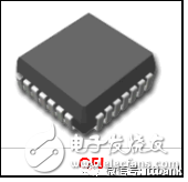
QFJ(quad flat J-leaded package)
Four-sided J-pin flat package. One of the surface mount packages. The pins are led out from the four sides of the package and are J-shaped downward. It is the name stipulated by the Japan Electromechanical Industry Association. The center of the pin is 1.27mm. The materials are plastic and ceramic. Plastic QFJ is often referred to as PLCC (see PLCC) for microcomputers, gate displays, DRAM, ASSP, OTP, etc. The number of pins is from 18 to 84. Ceramic QFJ is also known as CLCC, JLCC (see CLCC). The windowed package is used for UV erased EPROM and microcomputer chip circuits with EPROM. The number of pins is from 32 to 84.
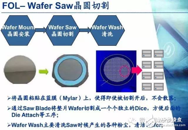
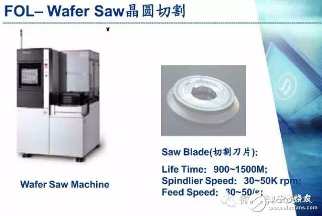
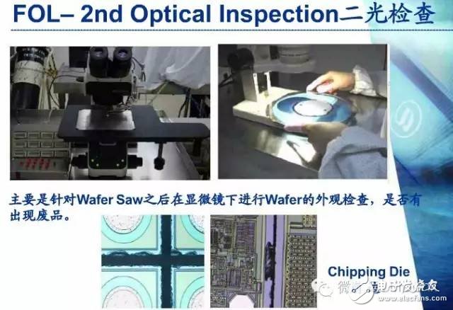
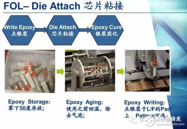
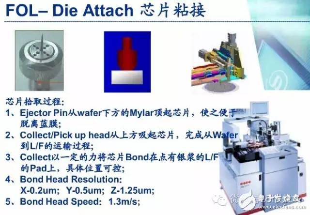
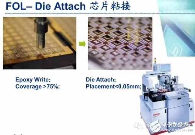
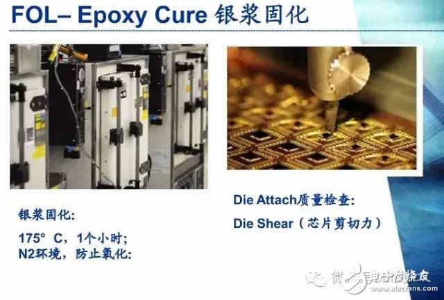
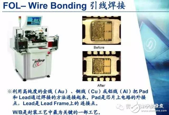
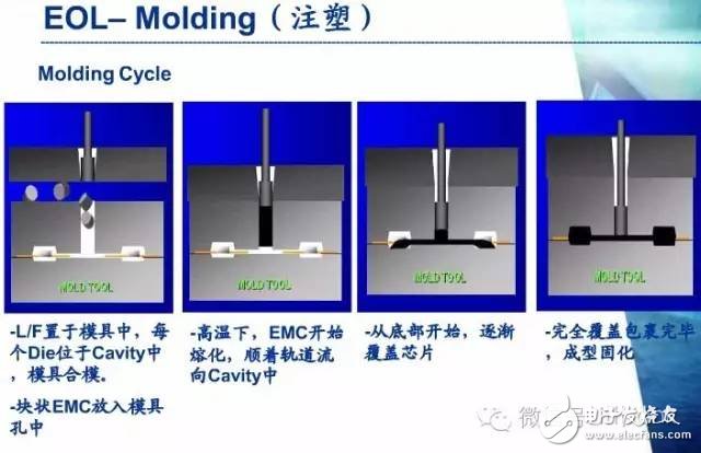
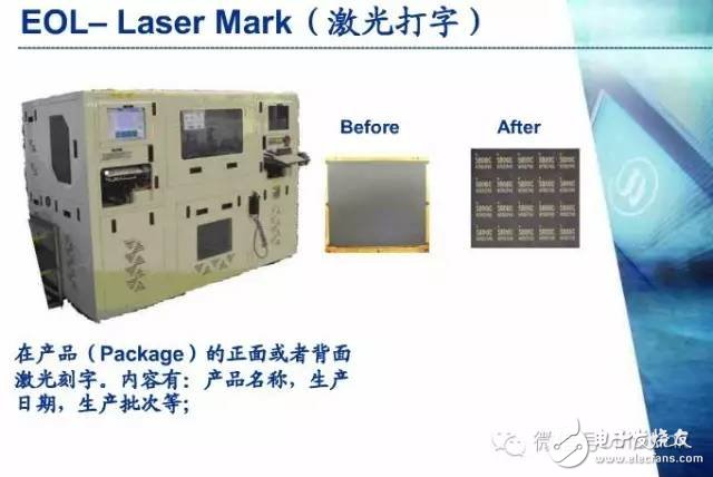
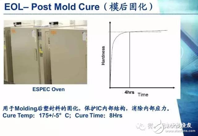
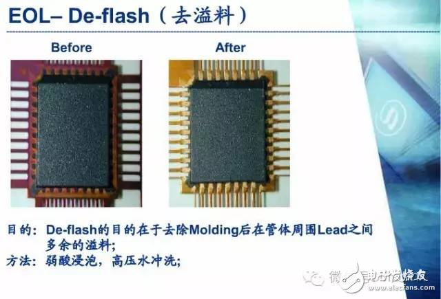
Package process details
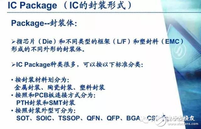
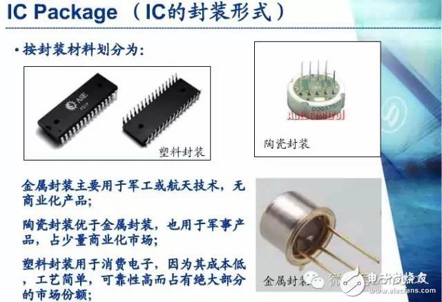
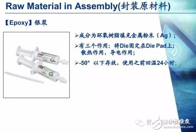
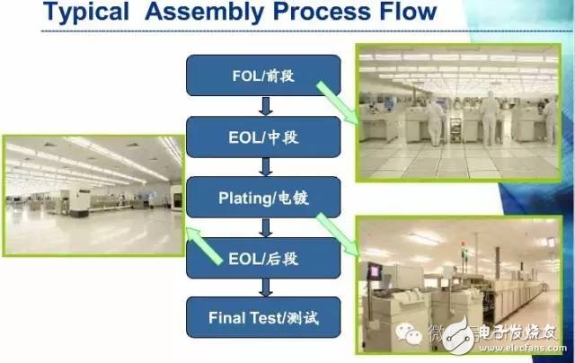
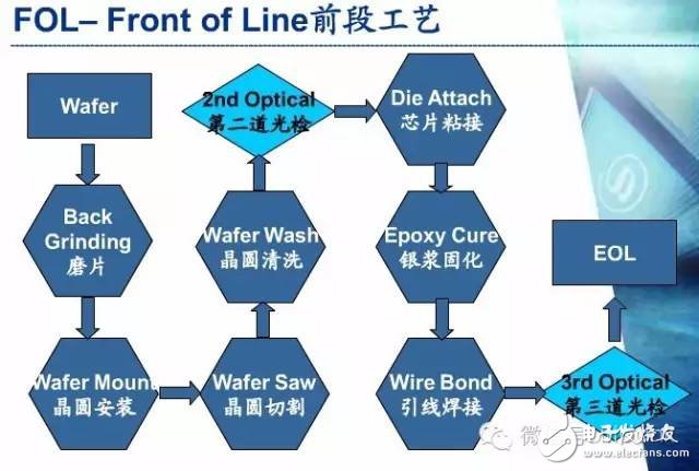
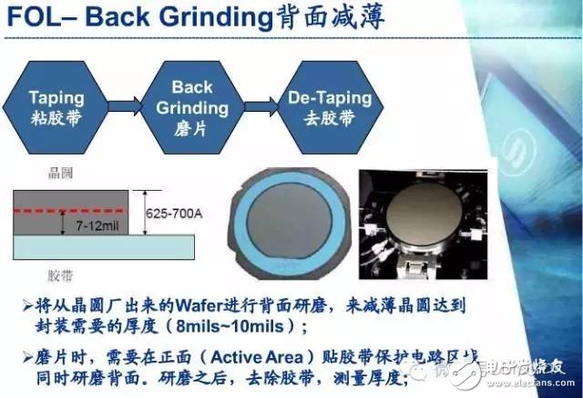

Standard Recovery Stud Diode are mainly used for rectifying and switching
It has positive pressure reduction (0.4v -- 1.0v), short reverse recovery time (2-10ns nanosecond), large reverse leakage current, low pressure resistance, generally lower than 150V, and is used in low voltage situations.
Diodes are electronic devices that have two electrodes that allow only a single current to flow in a single direction.Varicap bond (bond) is an electronic adjustable capacitor.Most diodes have a current orientation that we call reading "rectifier".The most common function of a diode is to allow only the current to pass in one direction (called forward bias) and to block in the opposite direction (called reverse bias).
Standard Recovery Stud Diode,Standard Recovery Diode,400V Standard Recovery Diode,Stud Diode
YANGZHOU POSITIONING TECH CO., LTD. , https://www.cnchipmicro.com