The basic composition and working principle of the pulse modulator
Circuit design
Waveform analysis and experimental testing
solution:Using a square wave generator 4060 and a trigger monostable flip-flop 74LS123 to generate a pulse period signal with adjustable pulse width
Pulse transformation and modulation pulse generation
With the development of millimeter-wave solid-state devices, millimeter-wave proximity detectors have gradually shifted from Ka-band to W-band. The application background of this paper is a W-band active-passive composite detector system, which is a micro-miniature detector that combines active millimeter-wave radar and passive millimeter-wave radiometer to measure, locate and target the target.
The pulse modulator is an important part of the system. In addition to modulating the RF power source, it also provides reference signals and trigger signals for the ranging circuit and signal processing circuit of the system. The RF power source of the system is generated by an avalanche diode oscillator. Compared with the body effect tube oscillator, the operating frequency is high and the power is high, but the transient driving current requirement of the pulse modulator is also high. The specific index requirements are: transient pulse current is not less than 15A, the power supply voltage is not higher than 25V, the pulse width is not more than 100ns, the pulse duty is less than two hundredth, and the rising and falling edges are about 10ns. The pressure drop rate at the top does not exceed 10%. The focus of this article is to study how to generate such pulses to meet system requirements.
The basic composition and working principle of the pulse modulator
The pulse modulator is mainly composed of four parts: a modulation switch, an energy storage element, a charging and isolation element, and a bypass element, as shown in FIG. 1 .
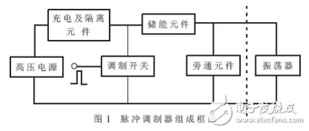
The functions of each part are as follows:
The charging and isolation components are both resistive and inductive. The function is to charge the energy storage component in a certain manner, and separate the high voltage power supply from the modulation switch to avoid overloading the high voltage power supply when the modulation switch is turned on.
The energy storage component is generally a capacitor with a large withstand voltage value and a large capacitance value. Its function is to take energy from the high voltage power supply during a long pulse interval and store it continuously, and transfer the energy to the oscillator during very short pulse operation. Thus, the power capacity and volume of the high voltage power supply are greatly reduced.
The bypass component is typically a resistor or an inductor. Its function is: the charging circuit constituting the energy storage element, when the energy storage element is discharged, the impedance it exhibits is much larger than the impedance of the oscillator, has no influence on the discharge current, and can also improve the waveform of the trailing edge of the modulated pulse.
The modulation switch uses a MOS power FET. Its function is to turn on the discharge loop of the energy storage element within a short time triggered by the external pulse to form a nanosecond modulation pulse, which is disconnected during the external pulse interval to charge the energy storage element. By abandoning the device such as the vacuum switch tube, the failure rate due to the failure of the vacuum device is reduced to zero, thereby improving the reliability of the detector and simultaneously reducing the volume of the detector.
Through the description of the functions of the above parts, it can be clearly seen that the working principle of the pulse modulator is to control the charge and discharge of the energy storage element by controlling the on/off of the modulation switch by using a pulse having a certain pulse width and a repetition period, thereby forming a conformity. The required high voltage pulse drives the oscillator to operate. It is essentially a power converter that converts a DC power source with a smaller average power into a narrow pulse source with a larger pulse power. Assuming that the energy stored in the energy storage element is Wc during the entire pulse interval, then Wc=Pe•(T-τ)•ηc (1)
Where, Pe is the average power supplied by the power supply; ηc is the charging efficiency; T is the pulse repetition period; τ is the pulse width.
In this system, T""τ, so T-τ≈T, then Wc≈Pe•T•ηc (2)
During the pulse period Ï„, the modulation switch is turned on, and the energy storage element is discharged to the oscillator load through the discharge loop to form a modulated pulse. Obviously, the power obtained by the oscillator during the pulse period Ï„, that is, the output pulse power PÏ„ of the pulse modulator is:

Where: ηd is the discharge efficiency; ηm=ηc•ηd is the efficiency of the modulator, generally 60% to 80%.
It can be seen from formula (4) that the pulse power of the modulator output is much larger than the average power supplied by the power supply modulator, and the power supply energy is fully utilized.
Circuit designa. Pulse control signal generation
There are many methods for generating periodic pulse signals by digital circuits. In this paper, a square wave signal with a period of 20μs is generated by the square wave generator 4060, and then the monostable flip-flop 74LS123 is triggered to generate a pulse with a pulse width of 50 ns to 150 ns. Periodic signal. The circuit schematic is shown in Figure 2.
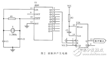
The 4060 is a 14-bit parallel binary counter with an oscillator. The counter counts when the falling edge of the clock arrives. The internal clock generation circuit can form an RC oscillator or a crystal oscillator through an external RC component or crystal. The output is The square wave signal can be used as the clock signal of the internal counter.
The 74LS123 is a commonly used one-shot, which can be used in a variety of trigger modes. It can be triggered by the rising or falling edge of the pulse signal to generate the required positive or negative pulse. The pulse width is determined by the value of the external RC. .
b. Pulse transformation and modulation pulse generation
Since the TTL level pulse signal output of the digital circuit is weak, it is impossible to directly drive a high-power MOS transistor, so the weak pulse signal must be amplified first to drive the latter MOS transistor. The amplification circuit is shown in Figure 3.
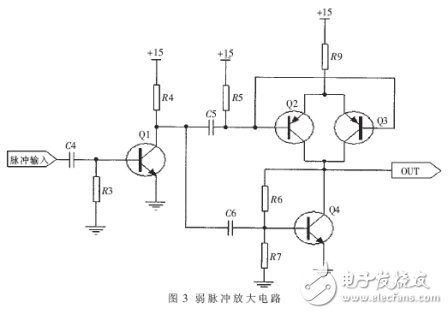
The output pulse of the weak pulse amplifying circuit controls the charge and discharge of the on-off control capacitor of the MOS transistor to form a modulated pulse that meets the requirements, and drives the oscillator to operate. The modulation pulse generation circuit is shown in FIG.
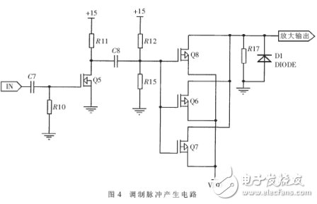
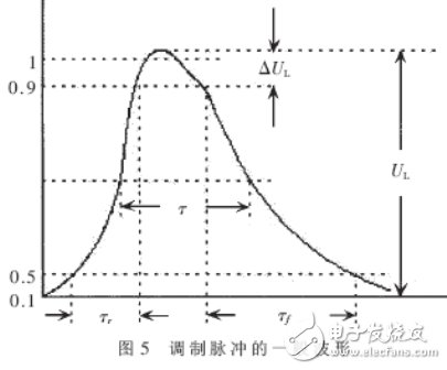
Ideally, the pulse output from the pulse modulator should be rectangular, the top of the rectangular pulse is flat, and the power and frequency of the avalanche tube oscillator are stable during the duration of the pulse. But in fact, because there are inevitably parasitic parameters in the pulse modulator, such as distributed capacitance, lead inductance, etc., the voltage and current on it cannot be abrupt, which makes it impossible for the pulse modulator to output the ideal rectangle. Modulation pulse, the general pulse waveform is shown in Figure 5.
In the figure, Ï„r represents the rising edge time of the pulse, Ï„f represents the falling edge time of the pulse, Ï„ represents the pulse width, and the rate of change of the top of the pulse is:

In the experiment, 1Ω pure resistance is used as the equivalent load, external 25V DC regulated power supply is used, and the output pulse waveform is observed with an oscilloscope. The output pulse waveform obtained on the oscilloscope is shown in Figure 6. In the figure, the abscissa is time, the unit is 100 ns/large grid; the ordinate is amplitude, and the unit is 5V/large grid. It can be seen from Fig. 6 that the pulse width is less than 100 ns, the rising edge time is less than 10 ns, the falling edge time is slightly larger than 10 ns, and the top is relatively flat. Since a 1Ω pure resistor is used as the equivalent load, the waveform can also be regarded as a pulse current waveform, from which it can be seen that the transient pulse current exceeds 15A.
The narrow pulse modulator developed in this paper is connected to an avalanche diode oscillator, which can oscillate the oscillator. The average power measured at 93.7 GHz output pulse is 9 dBmW, which indicates that the pulse modulator developed in this paper is feasible. The modulator can also be used to drive a Ka-band FET oscillator or a transmitter such as a pulsed millimeter-wave radar.
Shenzhen Kate Technology Co., Ltd. , https://www.katevape.com