In the aircraft launch test, the commonly used telemetry system obtains the working state parameters and environmental data of each internal system to provide a basis for assessing the performance and fault analysis of the aircraft. The digital converter is an important device on the telemetry system. Its main function is to control various flight parameters on the receiving missile. The performance of the converter will directly affect the telemetry results, which will have a great impact on the test data during the development and test of the aircraft. It will be related to the success or failure of the aircraft test and the improvement and improvement of the performance of the aircraft in the future. During the development of the aircraft, multiple tests and assessments are very important. Accurate, objective and reliable evaluation of digital converters is a key part of the production process, and this can only be done by the converter test system. Programmable logic devices (FPGAs) have gained wider and wider applications in modern test systems due to their high speed, reconfigurability, flexible design, low development cost, I/O pins and rich internal resources. This paper uses FPGA as the logic control center to design the test system, mainly for the unit test of the digital converter, which plays a key role in its actual development and debugging process.
System structure and working principle
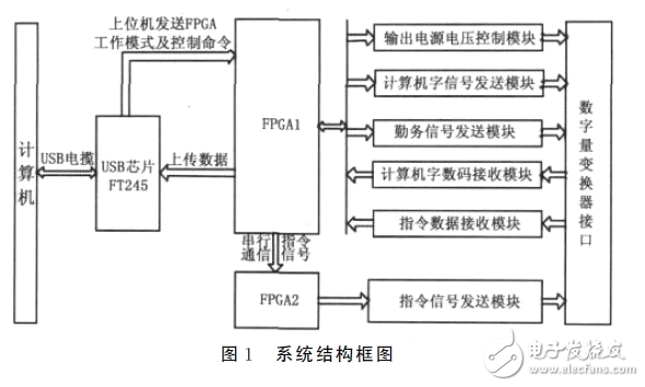
When designing the system, adopting the idea of ​​modular design, designing each functional module according to technical indicators, and completing the test task of the system through coordination and cooperation between the modules. The overall structure of the system is shown in Figure 1. The whole system consists of computer, USB chip FT245, two FPGAs, output power voltage control module, computer word signal sending module, service signal sending module, computer word digital and command digital receiving module. The command signal sending module is composed. The modular design enables simple and fast positioning and problem solving during system commissioning and hardware programming.

The hardware circuit selects XC3S200-208 and XC2S100-208 of XILINX Company as the logic control center of the system. XC3S200-208 is used as the main control chip, which mainly realizes command receiving and judgment of the host computer, and then generates and sends computer word signals. Receive computer word digital and instruction digital and frame and upload data to the host computer; XC2S100-208 acts as the slave control chip and completes the transmission of 128 command signals; the two FPGAs use serial communication to send control commands to achieve communication. In addition, the host computer software can be used to send reset or stop commands to the system, which can reduce the power consumption of the hardware and improve the working efficiency of the test system.
USB interface module implementation
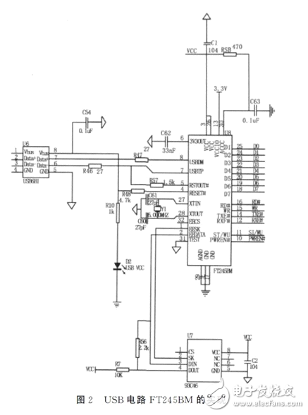
USB has the characteristics of low cost, good versatility, simple connection, and support for hot plugging. From the actual rate transmission requirements of the system, the design uses the universal USB interface chip FT245BM to communicate with the host computer. The main function of FT245BM is to realize data string/bidirectional conversion under the action of internal logic. Its maximum transmission rate can reach M/s. FT245BM eliminates complex firmware programming and driver writing, which can simplify USB interface design. , saving design time for the system.

The FT245BM's 8-bit data lines D7~D0, read signal RD, write signal WR, transmit enable TXE, and receive data completion signal RXF are connected to the FPGA to complete the communication between the two. The computer sends the control command signal to the FT245BM through the effective cooperation of the application and the dynamic link library. The FPGA receives the issued control command or sends the uploaded test data by using the I/O port connected thereto.
Output power voltage control module implementation
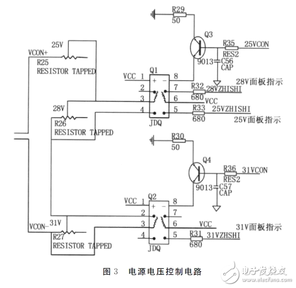
Since it is necessary to provide 3 working voltages of 25V, 28V and 31V for the digital converter to be tested, three kinds of resistors with different resistance values ​​can be connected at the output end of the power module, and the three kinds of voltages can be switched. The circuit for realizing the control is shown in Fig. 3. Shown.

In the figure, VCON+ and VCON- are the input voltages of the power module, and R25, R26 and R27 are used to adjust the resistance. 25VCON and 31VCON are connected to the I/O of the FPGA respectively. They are the control signals given by the FPGA. The function of the triode in the circuit is to increase the driving capability of the signal by using its current amplification. The control of the 3 command voltage is realized by the judgment of the control command by the FPGA. In addition, the system's default and reset output voltage is 28V.
Bluetooth Mini Projector
Sound can be transmitted wirelessly, no audio source cable is required.
1. The Bluetooth function of the projector can be connected to a Bluetooth speaker, and you can enjoy better sound quality when watching movies and playing music;2. After the projector is connected to the mobile phone through the Bluetooth function, the projector acts as a speaker and can play music from the mobile phone.
wifi bluetooth projector,bluetooth home projector,bluetooth protable home projector
Shenzhen Happybate Trading Co.,LTD , https://www.szhappybateprojector.com