FPGAs have to replace ASICs, which is the slogan that FPGA vendors have called for more than a decade. However, FPGA sites accounted for a lot, and ASIC still enjoyed it. What are the two brothers in the end? Field-Programmable Gate Array (FPGA), which is a field-programmable gate array, is a product further developed on the basis of programmable devices such as PAL, GAL, and CPLD. It emerged as a semi-custom circuit in the field of application-specific integrated circuits (ASICs), which not only solves the shortcomings of custom circuits, but also overcomes the shortcomings of the limited number of original programmable device gates. It is the main hardware platform for digital system design today. Its main feature is that it is completely configured and programmed by the user through software to complete a specific function and can be erased repeatedly. In the modification and upgrade, there is no need to change the PCB board additionally, just modify and update the program on the computer, make the hardware design work become the software development work, shorten the system design cycle, improve the flexibility of implementation and reduce the cost. .
An ASIC (Application Specific Integrated Circuit) is an integrated circuit designed for a specific purpose. Refers to integrated circuits designed and manufactured to meet the needs of specific users and the needs of specific electronic systems. ASIC is characterized by the needs of specific users, ASIC is divided into full custom and semi-custom. The highlight is dedicated, tailored so the execution speed is faster. In one sentence, the chip is not available on the market. The fruit's A-series processor is a typical ASIC.
FPGA is reusable
FPGA adopts the concept of logic cell array (LCA), which includes three parts: configurable logic module CLB, output input module IOB and internal connection. Field Programmable Gate Arrays (FPGAs) are programmable devices. The FPGA uses a small lookup table (16 × 1 RAM) to implement the combinational logic. Each lookup table is connected to the input of a D flip-flop. The flip-flop drives other logic circuits or drives I/O. The logic function, in turn, implements the basic logic unit modules of the sequential logic functions that are interconnected or connected to the I/O modules using metal wires. The logic of the FPGA is realized by loading programming data into the internal static storage unit. The value stored in the memory unit determines the logic function of the logic unit and the connection mode between modules or modules and I/O, and finally determines What the FPGA can do.
Features of FPGA: When power is applied, the FPGA chip reads the data in the EPROM into the on-chip programming RAM. After the configuration is completed, the FPGA enters the working state. After the power is turned off, the FPGA is restored to a white chip, and the internal logic relationship disappears. Therefore, the FPGA can be used repeatedly. In theory, FPGAs allow unlimited programming. The FPGA programming does not require a dedicated FPGA programmer, just a general EPROM, PROM programmer. There are a wealth of flip-flops and I/O pins inside the FPGA. Fast finished products can be modified to correct errors in the program and cheaper costs.
Users do not need to intervene in the layout and routing of the chip, and can change their logic functions at any time, flexible use.
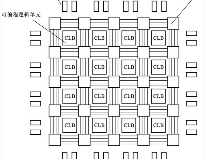
Figure FPGA Basic Architecture ASIC is customized for VIP services, which are divided into full customization and semi-custom. Full custom design allows for the smallest area, optimal layout, optimal power dissipation, and best electrical characteristics. Features: fine workmanship, high design requirements, long cycle, and expensive design.
The semi-custom design method is further divided into a standard cell-based design method CBIC and a gate array-based design method. Semi-customization is mainly suitable for small-scale digital circuit design with short development cycle, low development cost, investment and low risk.
The characteristics of ASIC are: for the needs of specific users, ASIC has the advantages of smaller size, lower power consumption, higher reliability, improved performance, enhanced confidentiality and lower cost compared with general-purpose integrated circuits in mass production. ASICs require a long development cycle and are highly risky. Once there is a problem, all the pieces are invalidated, so small companies can't afford it.
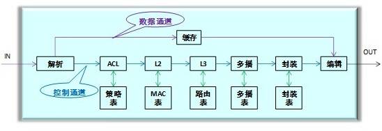
Figure ASIC basic architecture design process
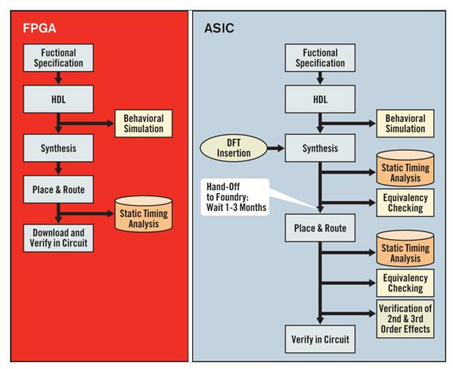
Figure FPGA and ASIC design flow
The complete FPGA design flow includes functional description, circuit design and input, functional simulation, comprehensive optimization, post-synthesis simulation, implementation and place and route, timing simulation, board level simulation and verification, debug and load configuration.
The ASIC design flow (digital chip) includes: function description, module division, module code input, module level simulation verification, system integration and system simulation verification, synthesis, STA (static timing analysis), formal verification.
To put it another way, in the ASIC design process, FPGAs are often used for prototyping. FPGA verification is an important part of ASIC design. Later, you need to introduce ASIC version source code, insert IO PAD, DFT, power estimation and other back-end processes. Completing the FPGA verification can be said to complete 50 to 80% of the entire ASIC process.
Considering the design cost, the FPGA is dominant in small batches, and the ASIC is dominant in large quantities.
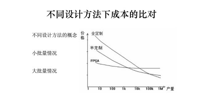
The FPGA itself is a chip, but you can programmatically modify internal logic connections and configurations to achieve the functionality you want. To implement an ASIC, just like starting with a blank sheet of paper, you have to have code, then synthesize, then layout, routing, and get the GDSII and then go to the stream. Specific speed
The same process and design, the speed on the FPGA should be slower than the ASIC. Because the FPGA is based on a general structure, that is, LUT (look up table), it can implement adder, combinatorial logic, etc., while ASIC, the general adder is the adder, and the comparator is the comparator, the FPGA structure Universality will inevitably lead to redundancy; in addition, as the basic unit of FPGA is LUT (LUT constitutes SLICE, SLICE constitutes CLB--this is the structure of xilinx), for this big design, if a LUT can't be realized, you have to use two LUTs. A SLICE can't be implemented with CLB. Different structures are in a specific position, and the interconnection between signals causes the wire delay to be a non-negligible part. There is no structural limitation for the ASIC, and it can be spatially close to a specific reality. In contrast, the wire delay and the cell delay should be smaller than the FPGA. Of course, there is also DFF in the LUT. As a high-speed design, it usually takes a shot after a simple combinatorial logic operation, and then does the next step.
Than a head
With the exact same structure, the FPGA is far away from the ASIC. FPGAs are much larger in size to achieve the same functionality as ASICs, with a fraction of the clock speed. Therefore, FPGAs are still much larger than ASICs.
Power consumption
Under the same process conditions, the FPGA is larger than the ASIC. FPGAs, especially those based on static memory (SRAM) look-up tables (LUTs) that occupy a large amount of silicon area and have six transistors per cell, and FPGAs that configure component technology consume much more power than equivalent ASICs.
It is more expensive than the silver FPGA of flowers, and the development tools and risks are basically non-existent. For the cost and development tools of ASICs, NRE costs become quite expensive as the process increases. Unless your chip is successful in mass production, the cost per piece will be extremely expensive! other aspects
ASICs are used for large projects, and FPGAs are more suitable for small projects that need to be quickly placed on the market and support remote upgrades. The main advantage of FPGA technology is still the short time to market.
In terms of the advantages of the ASIC, the ASIC can be run immediately after power-up, with more package options in terms of unit logic size, and some analog logic. In contrast, the FPGA load configuration takes time to enter the memory and therefore does not work immediately. In addition, the packaging of the FPGA is also more complicated.
In addition, the FPGA also includes interface I / O, I / O is divided into common I / O and high-speed I / O, high-speed I / O support such as high-speed SERDES, for high-speed interfaces such as XAUI, PCIE, etc. The interface is moving from a few Gbps to more than 10 Gbps. In addition, a variety of hard IP is also a differentiated competitive tool for FPGA vendors, such as POWERPC, ARM and other hard IP. Thus, the CPU+FPGA is integrated into a programmable programmability and reconfigurable processing platform. Therefore, compared with the past, FPGA has developed for 20 or 30 years, and its basic architecture has remained unchanged. Positioning of the two
The use of FPGA and ASIC products should be selected according to the positioning and design needs of the product. ASIC products are suitable for design scales such as CPU, DSP or multilayer switch chips, or for applications with very mature technology and very low profit margin. Products, such as household appliances and other consumer appliances, are also common devices such as RAM and PHY for a large number of applications. The FPGA products are suitable for products with moderate design scale, fast requirements for product market, or feature design with flexible product changes, such as PDH, SDH devices below 2.5G and most interface conversion chips. Of course, the specific use of that product to design must also be decided by the designer to fully consider their product positioning.
The two are beginning to integrate FPGAs in the most obvious combination of processors, and programmable ASICs are beginning to emerge. As the SoC becomes mainstream, the boundaries between the two are not so obvious. Finally, the netizens explained that FPGAs are faster than ASICs. The resources such as LUTs of FPGAs have been fixed. You don’t have to use them, no more. In ASIC theory, every resource you use such as CELL or IP can be manually placed for optimization. There are two disadvantages to FPGA resource fixation: Disadvantage 1: The resources that can be utilized are fixed and not large, and the logic that spans the area will degrade the timing. In fact, you have no way to put the logic as close as possible. Logic is close enough to reduce the delay on the line and increase the speed. You can squeeze all the ASIC cells together (without violating DRC). As shown in the figure below, this is a resource map of an FPGA.
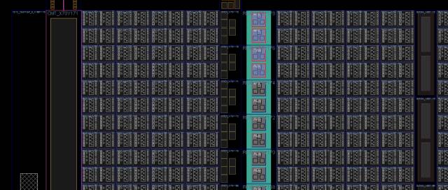
Disadvantage 2: Your size is fixed. Whether you use 1 door or 10W doors, it is the LUT that has been fixed for you. If your logic is very small, the FPGA is very large, and your signal comes from the IO into the logic, it may take a long distance, this will take time. In the extreme case, you come in from the upper IO, your logic is in the lower part, and the length of this line is touching. (Normal design won't do this)
In addition, the routing of the FPGA, you are almost unable to move.
In ASIC you can directly widen the metal lines, such as double the width of the clock line, reset the line, and the like. The width of the wire becomes larger, and the delay on the wire becomes smaller, which is also helpful for speed. Also, the asic library generally includes high-performance cells, low-power cells, and so on. In the critical path, in order to improve timing, you use high-performance cells (large power consumption). The general path, the timing is looser and more low-power cells (low performance). Once your FPGA is selected, you only have what he has given you, and you have not chosen it. ASICs can also use useful skew to increase speed, more than in FPGAs. In general, it is just like the GPU and CPU. The GPU can process images very quickly, but let the GPU handle other things, and the GPU stands by. A lot of CPU operations can be processed, and images can be processed, just slow. Once you are going to a certain purpose (ASIC), you can achieve this goal, you can not go offline. If you want to take care of all aspects (FPGA), you can't do it best in every aspect, you have to trade-off. Today's point of view is just a word, welcome everyone to make a brick.
Audible and visual alarm is set up to meet customers' special requirements for alarm loudness and installation location. At the same time, two alarm signals, sound and light, are issued. Special fields: iron and steel metallurgy, telecommunication towers, hoisting machinery, construction machinery, ports, transportation, wind power generation, ocean-going ships and other industries; it is an accessory product in the industrial alarm system.
emergency alarm,Audible Visual Signals,Visual Alarm devices,sound and light siren,visual alarm system
Taixing Minsheng Electronic Co.,Ltd. , https://www.ms-speakers.com