The remote communication system and remote monitoring system have two requirements for signal transmission: on the one hand, it requires flexible interfaces and high data transmission bandwidth; on the other hand, it requires the system to have a long transmission distance. Traditional interfaces such as UART, USB, Ethernet, etc. cannot meet the requirements in terms of transmission bandwidth and transmission distance.
Low-voltage differential signaling (LVDS) is a low-swing differential signaling technology. The constant current source mode and low swing output of LVDS enable the transmission speed to be from hundreds of Mb/s to more than 2 Gb/s. The differential transmission mode makes the LVDS signal more resistant to common-mode input noise. LVDS technology has low power consumption, and the power consumption of a 100Ω load resistance is only 1.2 mW. These characteristics make LVDS technology widely used in many fields that require high speed and low power consumption.
With the advancement of semiconductor technology, the performance and integration of Field Programmable Logic Arrays (FPGAs) are continuously improving, while costs are decreasing. FPGA on-chip resources are rich and flexible. By configuring logic resources and I/O, interfaces that support various standards can be generated, which is suitable for completing communication between interfaces. The reconfigurability of FPGA enables the same hardware environment to implement different functions, saving the cost of system upgrades and changes.
1 System composition and principleThe principle block diagram of the high-speed data transmission system is shown in Figure 1. The whole system consists of three parts: sending board, receiving board and transmission line.
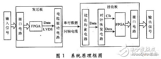
The sending board is mainly composed of an interface circuit, an FPGA and a cable drive circuit, and the completed function is to convert various input signals into serial data frames for transmission through the transmission link. The receiving board is mainly composed of a receiving equalization circuit, a clock recovery circuit, an FPGA and an interface circuit, and realizes the function of receiving and recovering the serial data frame into the original signal. The transmission line uses coaxial cable. Compared with twisted pair, coaxial cable has strong anti-interference ability and long transmission distance, and the cost of coaxial cable is lower than optical cable. The coaxial cable is suitable for the application of this system where the transmission rate is less than 200 Mb/s and the transmission distance is less than 300 m.
The input signal of the system includes serial port signal, network signal and parallel video signal, etc. Select MAX232, RTL8201, SN74LVC4245 and other chips to form the interface circuit respectively, and convert the input signal into LVTTL/LVCMOS level signal supported by FPGA, which plays a role in protecting the device and increasing the signal driving capability.
The FPGA on the receiving board first completes the reception of system input signals, and then converts the signals in the asynchronous clock domain to the unified system clock, and then converts the signals in parallel to serial and adds the start bit, stop bit and check bit to form a specific frame Format, and then encode it with 8 B/10 B, and finally output with LVDS level through differential I/O. The receiving board FPGA decodes and deframes the signal after receiving the serial signal, extracts the original data for restoration, and finally outputs the restored signal to each interface through the corresponding I/O.
The transmission distance of the LVDS signal directly output from the FPGA is less than 10 m at a transmission rate of 100 Mb/s. It is necessary to use a cable drive circuit to increase the drive capacity of the LVDS signal. At the same time, a receiving equalization circuit is used to compensate for the attenuated signal after transmission through the cable, so as to strengthen the system. The purpose of long-distance transmission capability.
If one coaxial cable is used to transmit the clock and the rest of the data is transmitted, the setup time and hold time of the received data cannot meet the requirements of the subsequent circuit because it cannot be guaranteed that these cables are strictly equal in length. On the other hand, the Jitter of the clock signal will increase after transmission, making the PLL inside the FPGA unable to lock the clock. All data signals are transmitted on the cable of this system, and the synchronous clock of the receiving end is restored from the serial data through a clock recovery circuit.
2 System hardware design 2. 1 FPGA partial circuit designThe system uses Xilinx's Spartan3 series FPGA: S3C500E. It has 10 476 logic units, 232 I/Os, 4 clock management modules (DCM), and the memory includes 360 Kb block RAM and 73 Kb discrete RAM. All I/Os can form 92 groups of LVDS differential pairs, and the highest input and output rate is as high as 622 Mb/s, so the system does not require additional circuits to implement LVDS interfaces. The DCM module can flexibly multiply or down the input clock, with a maximum operating frequency of 311 MHz. The above parameters and performance not only meet the current design requirements, but also reserve sufficient design margin for system upgrades. The FPGA peripheral circuit includes a clock part and a configuration part. The clock is provided by the crystal oscillator on the circuit board and is connected to the FPGA through the GCLK pin. GCLK is a dedicated clock pin, this pin has a strong driving ability, and the delay to all logic units is basically the same. The configuration circuit adopts active SPI mode. Compared with other modes, the peripheral circuit of the active SPI mode is simple, small in size and low in cost. Moreover, SPI FLASH has a large capacity, in addition to storing configuration files, it can also store other user data. The configuration file size of S3C500E is 2 Mb, and this system uses M25P16 with a storage capacity of 16 Mb as the configuration memory.
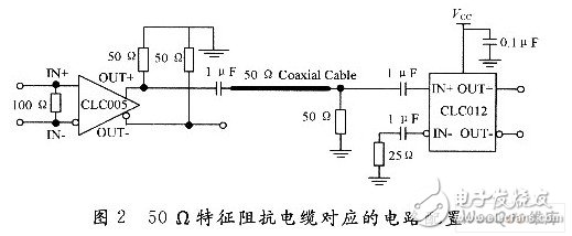
2.2 Transmission part circuit designThe design of the transmission part includes selecting the coaxial cable and designing the corresponding transmitting and receiving circuit. The type of coaxial cable used in this system is SVY-50-3, which has low cost and good performance. The characteristic impedance of this cable is 50 Ω, and the maximum attenuation of signal transmission 100 m at a rate of 150 MHz is 18.01 dB. It has good shielding characteristics and can work normally in a complex electromagnetic environment. The cable driving circuit and the receiving equalization circuit are respectively selected from National Semiconductor's chips CLC005 and CLC012. CLC005 supports LVDS level input, the highest transmission rate reaches 622 Mb/s, and the output signal peak-to-peak value ranges from 0. 7~2 V. CLC012 can automatically equalize signals with a frequency between 50 and 650 MHz. The clock recovery device selects CLC016, its input signal comes from CLC-012, the output clock and data are connected to FPGA, and the recovered clock is valid on the rising edge of the data. CLC005 and CLC012 are used in transmission systems with a characteristic impedance of 75 Ω. For this coaxial cable with a characteristic impedance of 50 Ω, the peripheral resistance configuration needs to be changed. Otherwise, the impedance mismatch will cause signal reflections, which will ultimately lead to the degradation of signal transmission quality. The corresponding configuration is shown in Figure 2.
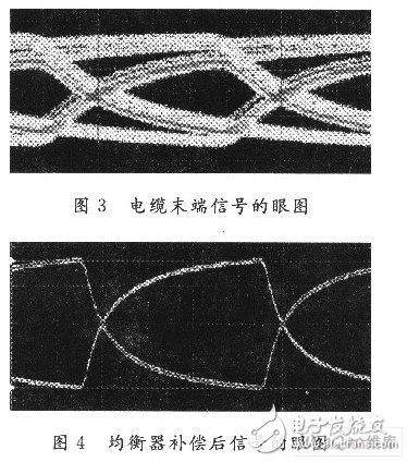
Through testing, this group of transmission devices can drive LVDS signals to transmit at least 200 m through SVY-50-3 type cables. After the signal is transmitted, the attenuation is serious at the end of the cable, and the noise and jitter are also serious. At this time, the signal eye diagram is shown in Figure 3, and it can be seen that the signal quality is poor. Receiving this signal directly will cause misjudgment of the signal level, and the jitter of the signal will cause the subsequent circuit to fail to work normally. After the receiving equalizer CLC012 automatically provides compensation for signal loss, the noise and jitter on the signal have been improved, and the eye diagram of the signal is shown in Figure 4.
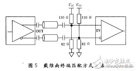
The LVDS driver is composed of a constant current source, so terminal matching is required. Normally, a 100 Ω resistor is connected in parallel at the input to meet the differential impedance required by the interconnected system. In a strong noise environment, the Thevenin terminal matching method can be used to provide a bias voltage of 1.2 V when AC coupling is connected, while meeting the design requirements of 100 Ω differential impedance. The specific method is to pull up the +/- end of the LVDS to VCC through a 130 Ω resistor, and pull down the 82 Ω resistor to the ground at the same time. As shown in Figure 5, the resistance accuracy is required to be 1%.
In the PCB design process, pay attention to the layout of the circuit board. The analog circuit and the digital circuit need to be separated and connected using a single-point grounding method. The VTTL/LVCMOS signal and the LVDS signal with fast edge rate change are arranged on different signal layers, and the power supply is separated from the bottom layer to reduce the crosstalk coupled to the LVDS line. LVDS wiring must follow the following rules:
(1) After the two signals of the differential pair fan out from the chip, they should be as close as possible (tightly coupled), which helps to eliminate reflections and ensure that the coupled noise is in common mode.
(2) The wiring length of the internal signal should be kept consistent to reduce the signal delay, and the length matching should be controlled within 10 mil.
(3) Maintain a fixed line spacing for internal signals to avoid discontinuity of differential impedance due to line spacing changes.
(4) Keep the differential pairs as far away as possible to reduce crosstalk between the lines. If necessary, place grounding vias for isolation between the differential pairs.
(5) Minimize the number of vias on the differential signal line, avoid 90° corners, and use circular arcs or 45° broken lines instead.
(6) The LVDS signal cannot be divided across planes, otherwise the impedance will be discontinuous due to the lack of a reference plane. A complete reference plane must be set for the LVDS signal.
(7) The matching resistance is as close as possible to the receiving end.
3 systematic logic design 3.1 Partial design of the clockThe clock signal is provided by a 40 MHz crystal oscillator on the circuit board. The 120 MHz system working clock is obtained by multiplying the DCM clock frequency by the digital clock management unit. When using the DCM module, note that the input and output of the DCM need to be connected to the global clock resource through the BUFG unit. The global clock resource is realized by the all-copper layer process, and a dedicated clock buffer and drive structure is designed to minimize the delay and jitter of the global clock reaching all logic units inside the chip. The DCM enables the LOCK signal after the clock is locked, indicating that the clock frequency multiplication work is completed, and uses this signal as a reset for other logic within the FPGA.
3.2 Asynchronous clock domain transformationThe system input signals work in different asynchronous clock domains, and the signals need to be converted to the same clock domain inside the FPGA.
The serial port signal speed is low, and the system clock can be collected at a high speed. According to the Nyquist sampling law, the sampling frequency is greater than 2 times the highest frequency of the signal, and the original signal can be restored from the sampled signal without distortion. This system uses a clock higher than 5 times the baud rate of the serial port to collect serial port data. After extensive testing by the BER tester, the serial port data can be correctly received and restored.
The video signal is a parallel signal, and the high-speed acquisition method will increase the amount of data, which is not suitable for this system. This system uses dual-port FIFO to complete asynchronous clock domain conversion. S3C500E's on-chip Block RAM resources can flexibly generate dual-port FIFO. Compared with dual-port FIFO generated by ordinary logic units, it has high stability, fast reading and writing speed, and low probability of generating a meta-stable state. The input end of the dual-port FIFO is connected to the clock and data of the system input signal; the output end is connected to the system clock data. The reading clock speed of the dual-port FIFO must be higher than the writing speed to avoid the loss of valid data due to overflow after the FIFO is full. On the other hand, when the slow clock domain is converted to the fast clock domain, the FIFO will appear to be read empty, and invalid data will be taken out at this time (the data is a repetition of the last data in the FIFO). Invalid data is transmitted to the receiving end through serial data frames, which will cause errors in the output signal after recovery. Therefore, the system adds the empty signal of the FIFO to the data frame to identify invalid data.
3.3 Data framing and codingSynchronous transmission requires the original data to be formed into a data frame and then sent, that is, a start bit, a stop bit and a check bit are added between the data. If the start bit of the data frame is too long, it will affect the transmission efficiency, and if it is too short, it will increase the difficulty of recognition at the receiving end. This system chooses 80 b as a frame, the start bit is 8 b, the stop bit is 2 b, and the odd parity bit is 1 b. The receiving end logic locates the start bit of the data frame after analyzing multiple data frames. Since the data length of each frame is fixed, after finding the starting bit of a certain frame, the starting position of each subsequent frame can be calculated periodically, and there is no need to repeat the identification work.
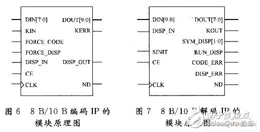
The average bit rate of the signal after data framing may be lower than the lowest operating frequency of CLC012, which cannot be directly used for transmission, and 8B/10B encoding is also required for it. The 8B/10B technology converts 8 data bits into a code of 10 data bits through a certain mapping mechanism, so that the number of "O" and "1" sent is consistent, continuous "1" or "0" Basically no more than 5 digits. The 8 B/10 B coding technology ensures the DC balance of transmission and increases the reliability of information transmission. The system uses the 8 B/10 B encoding and decoding IP core provided by Xilinx, which reduces the development cycle of the system and increases the stability of the system. Figure 6 and Figure 7 show the schematic diagrams of the module of 8 B/10 B encoding and decoding IP.
A high-speed communication system based on FPGA is introduced, which expands the transmission distance of LVDS signals through a cable driver and a receiving equalizer. After testing, the transmission distance using coaxial cable reaches 200 m, and the transmission rate of a single channel reaches 120 Mb/s. The reconfigurability of FPGA makes the system flexible and changeable and can adapt to different application requirements.
9000Puffs Disposable Vape,9000Puffs Disposable Vape Device,Vape Pen 9000Puffs,R&M 9000Puffs Vape Device
Shenzhen Uscool Technology Co., Ltd , https://www.uscoolvape.com