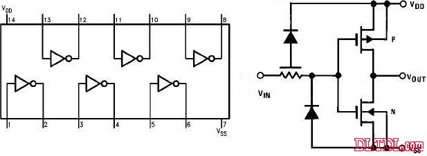
The CC4069 consists of six COS/MOS inverter circuits. This device is primarily used as a general purpose inverter, in circuits that do not require medium power TTL drive and logic level shifting.

CD4069 pin function diagram

AC test circuit and waveform switching time
Absolute Maximum Ratings Absolute Maximum Ratings:
DC Supply Voltage DC Supply Voltage (VDD) -0.5V to +18 VDC Input Voltage Input Voltage (VIN) -0.5V to VDD +0.5 VDC Storage Temperature Range Storage Temperature Range (TS) -65°C to +150°C Power Dissipation Power Consumption (PD) Dual-In-Line Normal Dual Row Package 700 mW Small Outline Small Outline Package 500 mW Lead Temperature Soldering Temperature (TL) Soldering, 10 seconds) (welding 10 seconds) 260°C
Recommended Operating Conditions Recommended Operating Conditions:
DC Supply Voltage DC Supply Voltage (VDD) 3V to 15VDC Input Voltage Input Voltage (VIN) 0V to VDD VDC Operating Temperature Range Operating Temperature Range (TA) -40°C to +85°C
DC Electrical Characteristics DC Electrical Characteristics:
Symbol symbol
Parameter parameter Conditionss condition -40°C +25°C +85°C
Units unit
Minimum and minimum typical maximum and maximum maximum IDD Quiescent Device Current quiescent current VDD=5V, VIN=VDD or VSS 1.0 1.0 7.5 μA VDD=10V, VIN=VDD or VSS 2.0 2.0 15 VDD=15V, VIN=VDD or VSS 4.0 4.0 30 VOL LOW Level Output Voltage Output low level voltage |IO| < 1μA VDD = 5V 0.05 0 0.05 0.05 V VDD = 10V 0.05 0 0.05 0.05 VDD = 15V 0.05 0 0.05 0.05 VOH HIGH Level Output Voltage Output high level voltage | < 1 μA VDD = 5V 4.95 4.95 4.95 V VDD = 10V 9.95 9.95 9.95 VDD = 15V 14.95 14.95 14.95 VIL LOW Level Input Voltage Input Low Level Voltage |IO| < 1 μA VDD = 5V, VO = 4.5V 1.0 1.0 1.0 V VDD = 10V, VO = 9V 2.0 2.0 2.0 VDD = 15V, VO = 13.5V 3.0 3.0 3.0 VIH HIGH Level Input Voltage Input High Voltage |IO| < 1 μA VDD = 5V, VO = 0.5V 4.0 4.0 4.0 V VDD = 10V, VO = 1V 8.0 8.0 8.0 VDD = 15V, VO = 1.5V 12.0 12.0 12.0 IOL LOW Level Output Current Output low level current (Note 4) VDD = 5V, VO = 0.4V 0.52 0.44 0.88 0.36 mA VDD = 10V , VO = 0.5V 1.3 1.1 2.25 0.9 VDD = 15V, VO = 1.5V 3.6 3.0 8.8 2.4 IOH HIGH Level Output C Urrent output high level current (Note 4) VDD = 5V, VO = 4.6V -0.52 -0.44 -0.88 -0.36 mA VDD = 10V, VO = 9.5V -1.3 -1.1 -2.25 -0.9 VDD = 15V, VO = 13.5 V -3.6 -3.0 -8.8 -2.4 IIN Input Current Input current VDD = 15V, VIN = 0V -0.30 -10-5 -0.30 -1.0 μA VDD = 15V, VIN = 15V 0.30 10-5
D-sub Connector Contacts
A D-sub connector is a form of connector commonly found in electronic and computer systems. It consists of a D shaped metal band and two or more parallel rows of either pin contacts (male) or socket contacts (female). D-sub connector contacts can vary in size, material, current rating, length and resistance.
The most common type of connector is the crimp contact. These are assembled by inserting a stripped wire end into the cavity at the rear of the contact. The cavity is then crushed using a crimp tool, gripping the contact to the wire.
What are D-sub connector contacts used for?
The D-sub connector contacts carry the signal from the source to the destination across the D–sub connection.
Types of D-sub connector contacts
Most D-sub connectors are supplied with contacts ready in place. Contacts can be replaced if damaged or if the application of the D-sub connector is to be changed from the original design specification.
High-current, high-voltage, or co-axial inserts require larger contacts. The material of the D-sub connector contact can be changed if the robustness or quality of the connection needs to be improved.
D-SUB coaxial contact,D-Sub Connectors Contacts,D-Sub Plug Connectors Contact,D-Sub Receptacle Connectors Contact
ShenZhen Antenk Electronics Co,Ltd , https://www.antenkcon.com