This article guides reading
Reliability is the soul of every product. If a product's reliability is not good, it is a failed product because customers will not use products with risks. However, the reliability of products is not only affected by internal factors such as power-on and power-off and resetting. It will also be interrupted by external factors such as the sudden shutdown of the power supply and the working environment. The reaction of the product's control system to sudden power failure and protection measures are important criteria for judging product reliability.
First, the importance and feasibility of system power-down protection
In the use or debugging of embedded system products, they often encounter sudden power loss of the system power. This sudden situation will cause the system to lose important data and cannot recover, and the system will abruptly stop during operation. The operating memory of SD card or SDRAM causes damage. This situation will often affect the reliability of the product. In order to avoid this instability situation as much as possible, the product needs to increase the power-failure detection and protection circuit.
The brownout detection and protection circuit monitors the system voltage. When the system voltage drops to the low voltage alarm value, the circuit will find and react and send a warning signal. The processor immediately saves the data after receiving the warning signal. To prevent system data loss.
Second, power failure detection protection circuit block diagram
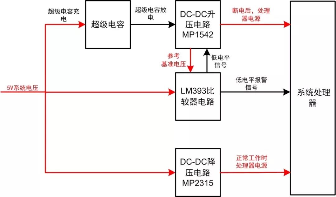
Figure 1 is a typical power-failure detection protection circuit. This functional block diagram allows everyone to better understand the working principle of the brownout detection protection circuit.
The power-down circuit has four parts: a super capacitor circuit (including a transistor switch circuit), a DC-DC boost circuit, a LM393 comparator circuit, and a DC-DC step-down circuit. This four-part circuit and processor form a complete brownout detection and protection circuit.

Figure 1 Power-failure detection circuit frame
Third, the use of LM393 comparator circuit
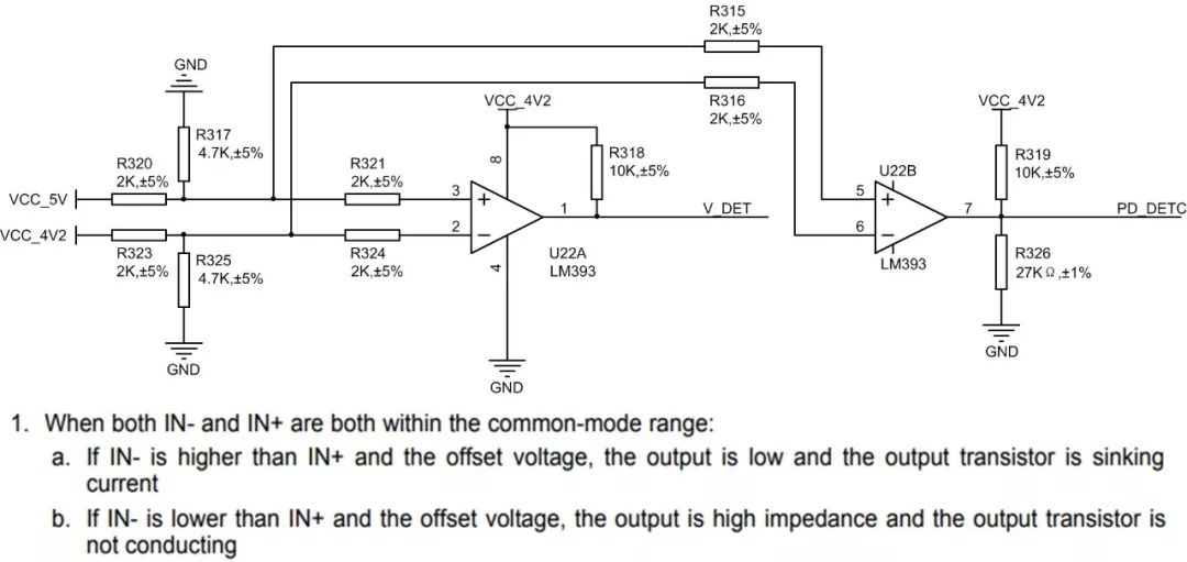
The LM393 comparator circuit is shown in Figure 2. The comparator IN- input VCC_4V4 is the output of the MP1542 boost circuit. The IN+ input is the system's 5V voltage. When VIN-> VIN+, the comparator output is low. When VIN-< VIN+, the comparator output is high.

Figure 2 LM393 comparator circuit
Fourth, the use of MP1542 boost circuit
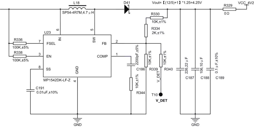
MP1542 boost circuit shown in Figure 3, the system through the LM393 comparator circuit controls the boost circuit enable:
After the system is powered on, the input values ​​at both ends of the comparator are as follows: VIN- <VIN+, so the comparator outputs a high-level signal, in which the V_DET signal is connected to the negative feedback terminal of the MP1542, and the V_DET is high, the output of the circuit is pulled low, reaching Does not enable boost circuit effects;
After the system is powered off, the 5V system voltage drops rapidly. The input values ​​at the two ends of the comparator are as follows: VIN->VIN+, so the comparator outputs a low-level signal and V_DET is low, according to the formula: Vout=[(12/5) +1] * 1.25, MP1542 circuit output 4.25V, to achieve the effect of enabling the boost circuit.

Figure 3 MP1452 circuit
Fifth, power failure detection and protection circuit power waveform and working process
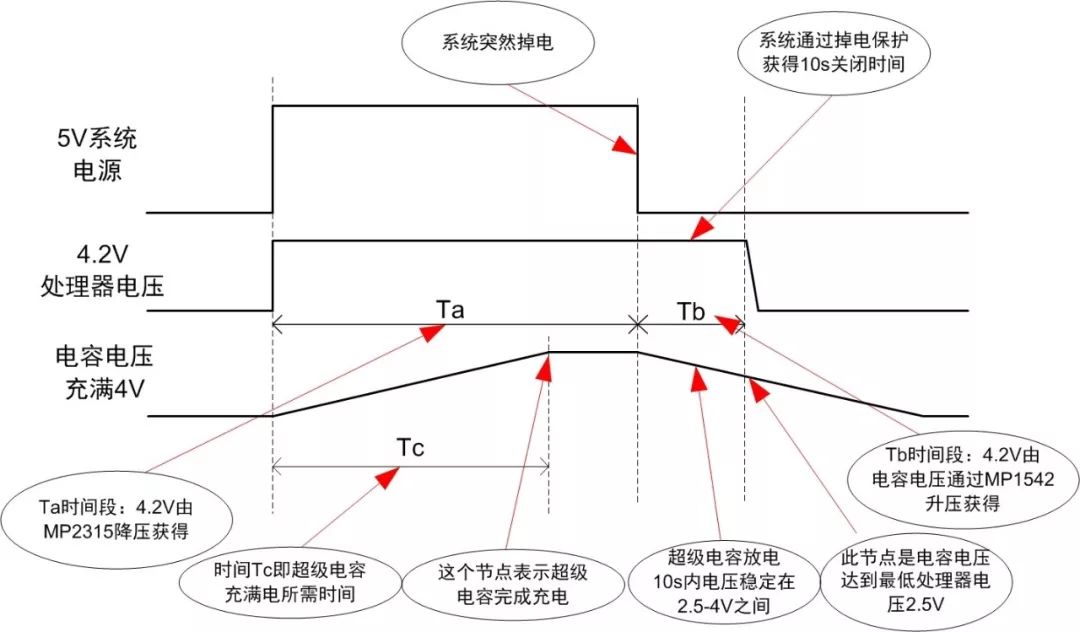
In order to understand the function of the power-failure detection and protection circuit more intuitively, we have plotted the power supply waveform diagram of the system operation. As shown in FIG. 4, the four parts of the power-failure circuit each play a different role at different times.

Figure 4 system power waveform
When the 5V power supply, 5V voltage to promote the transistor switch circuit conduction, LM393 comparator high output makes the MP1542 boost does not work for the super capacitor to provide only into the charging environment (capacitor is full after the voltage is 4V ), The system's commonly used 4.2V power supply is 5V obtained through MP2315 step-down circuit.
When the system is powered off, the low-level signal of the LM393 comparator enables the MP1542 circuit to provide a discharge loop for the supercapacitor (capacitor voltage is stable at 2.5-4V for 8-10S, minimum output voltage is 2.5V for MP1542), and the capacitor voltage passes through MP1452 circuit rises to 4.2V, as a standby power supply for the processor. When the standby power is turned on, the LM393 comparator also sends a low level alarm signal to the processor. As shown in Figure 2, the PD_DETC signal is directly output to the processor. The processor detects this signal and immediately saves data and a series of emergency operations to shut down the system.
When using this circuit, you need to pay attention: before the voltage across the super capacitor does not reach 2.5V, the power-failure detection and protection circuit can not work normally, so the capacitor charging time needs to be controlled. The charging formula of the super capacitor is: t = (C * V)/ I, C is the rated capacity of the supercapacitor, V is the operating voltage of the supercapacitor, I is the charging current, the charging time of the supercapacitor can not be too long, will affect the performance of the system.
The above article describes the circuit is a very useful system power-down detection and protection circuit, this circuit can make embedded systems to avoid sudden loss of power when the phenomenon of data loss, effectively improving the reliability of the product.
Din Rail Connectors,Din Terminal Block,Din Rail Mount Terminal Block,Rail Terminal Block
Cixi Xinke Electronic Technology Co., Ltd. , https://www.cxxinke.com