The JESD204B is the latest 12.5 Gb/s high speed, high resolution data converter serial interface standard. The converter manufacturer's related products have entered the market, and products supporting the JESD204B standard are expected to be available in the near future. The primary value of the JESD204B interface is its ability to reliably increase the data transfer bandwidth between the converter and logic devices such as FPGAs or ASICs.
Like any new interface, JESD204B brings new challenges. For system developers, the challenge is how to achieve optimal deployment of JESD204B from a PCB design perspective and how to debug the system after a problem. For component manufacturers, the challenges they face include testing the new JESD204B device. Testing not only ensures that the device meets specifications in a relatively ideal environment, but also ensures that the JESD204B device will function properly in the final system environment.
This article discusses the JESD204B specification, reviews the tests required to validate the JESD204B device, and lists ways to reproduce the final system environment.

JESD204B—The natural evolution of data converters From audio and music to test instrumentation, data converters (digital-to-analog converters and analog-to-digital converters) are used in many applications. Data converter products are constantly evolving. As bit depth and sampling rate increase, data input and output become more and more difficult. A decade or two years ago, the sampling rate of high-speed converters did not exceed 100 MSPS, so using a TTL or CMOS parallel data bus would suffice. For example, a 12-bit converter that integrates 12 data-dedicated pins can be set to have an appropriate setup and hold time relative to the clock.
As the speed exceeds 100 MSPS, this single-ended signal setup and hold time can no longer be maintained. To increase speed, high-speed converters use differential signals, but at the cost of more pins. For example, a 12-bit converter would then need to provide 24 dedicated pins for data. In order to solve the problem of the number of pins, a serial data interface was introduced. The converter's 6&TImes; serial data interface now requires only two differential I/Os (only 4 pins) for data transfer from the same 12-bit converter. With the rapid development to date, the data interface of the data converter has been developed using the JESD204B specification.
The JEDEC standards organization has released two versions of the JESD204 high-speed serial digital interface specification. The JESD204 2006 specification is the first release that brings the benefits of the SerDes high-speed serial interface to data converters with a maximum rated speed of 3.125 Gbps. This release released a revised version (JESD204A 2008 specification) in 2008 with the addition of important enhancements, including support for multiple data channels and channel synchronization. JESD204B is the second version of the specification developed by the International JEDEC JC-16 Task Force (Project: 150.01), which consists of approximately 65 members from 25 companies. It offers a range of major enhancements including higher maximum channel rates, deterministic latency support through the interface, and support for harmonic frame clocks.
Lack of official compatibility test specifications Unlike many other high-speed serial interface standards, the JESD204B standard does not contain official compatibility test specifications. The test specification is extremely valuable because it lists the tests that must be performed to ensure compatibility, as well as the test steps. Allowing different manufacturers to use uniform steps helps ensure consensus on the specification and eliminates hypothetical differences. But the lack of an official compatibility test specification does not mean that everything is missing. Everything you need to develop a set of tests and procedures is included in the JESD204B specification and in the corresponding specifications. Each chip manufacturer and system developer needs to collect this information.
Physical Layer Testing Physical layer (or PHY) testing is related to each data channel driver and receiver circuit: in other words, it is a link test. They do not include digital functional testing or procedural testing. A recommended list of SerDes PHY tests can be obtained from Section 1.7 of the OIF-CEI-02.0 specification when developing a complete PHY test list. The JESD204B specification strictly follows these recommendations, but has been partially modified. For example, JESD204B does not specify random jitter as an independent test item, but instead includes it in the total jitter. In addition, JESD204B specifies JSPAT, JTSPAT, and modified RPAT as the recommended test pattern, while the OIF-CEI-02.0 specification uses the PRBS31 pattern.
In addition to the required PHY tests, additional PHY tests can be performed - some of the OIF-CEI-02.0 specifications or tests not listed in the PHY portion of the JESD204B specification. For example, you can refer to other SerDes compatibility test specifications and use tests such as internal skew (for Tx) and internal skew tolerance (for Rx). These are not mentioned in order to recommend incorporating these tests into the JESD204B specification, as there is no need for additional PHY testing to ensure JESD204B compatibility; the purpose of mentioning this is to remind people that if a PHY test fails, other PHY tests can be used. To help understand the reasons for the failure.
After determining the test list, restrictions on these tests can be obtained from the JESD204B specification. Just remember that there are three types of limitations: LV-OIF-11G-SR, LV-OIF-6G-SR, and LV-OIF-SxI5. A particular JESD204B device can support multiple limitations. In this case, all restrictions supported by the component should be tested.
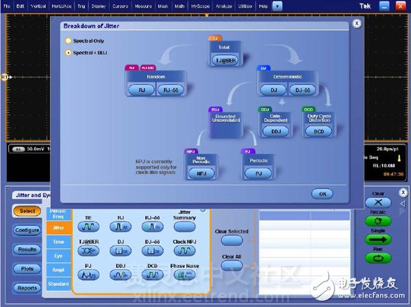
One type of confusion that can be generated by the JESD204B PHY test is related to the jitter terminology. The JESD204B and OIFCEI-02.0 specifications use different terminology, and the terms used by different test equipment vendors are also different. A typical jitter diagram is shown in Figure 1. The test equipment manufacturer's terminology is based on the industry standard dual Dirac jitter model. This difference in terminology can affect test steps, and jitter is a very difficult problem. Table 1 shows the jitter terms we translate (the jitter terminology used in the JESD204B specification differs from the test equipment vendor).


Figure 1. Typical jitter diagram, including identifying bounded uncorrelated jitter (BUJ)
Another area of ​​confusion for the JESD204B PHY test is the eye mask with a data rate of over 11.1 Gbps. In the JESD204B specification, for data rates above 11.1 Gbps, a 11.1 Gbps normalized bit time should be used. Therefore, if the operating rate is 12.5 Gbps (bit period is 80 ps), a 11.1 Gbps (90.9 ps) bit period should be used. The problem here is that the eye mask can start at the edge of the UI or it can start at the center of the UI, and JESD204B does not explicitly define its starting reference point. If the reference point is the UI center, the eye mask is larger than usual under 12.5 Gbps, so Tx is not easy to pass, but it is convenient for Rx to work. If the reference point is the UI edge, the eye mask is smaller than usual at 12.5 Gbps, so Tx is easier to pass, but it is not conducive to Rx work. Before this issue is resolved, it is recommended to test the two eye mask options separately to ensure compatibility.
Timing testing lists the complete timing test list for JESD204B is very difficult. At least a dozen timing diagrams have been defined throughout the specification, and the timing of the respective Tx, channel or Rx cannot be determined very quickly. In addition, some timings only apply to specific subclasses (0, 1, or 2). If you simply integrate timing specifications into a single table, the official compatibility test specification will play a big role. As long as you spend some time systematically understanding these timing specifications, there is no confusion.
For system developers, the good news about timing is that it's easier to set timing for JESD204B components than to get relevant information directly from the specifications. For subclasses 0 and 2, simply specify the device's clock to SYNC~ timing. For subclass 1, simply specify the device's clock to the SYSREF timing.
Protocol Testing For PHY testing, there is no official JESD204B protocol test list. Therefore, users need to browse the specification content and write a list of functions to be tested. This section lists a large number of recommended protocol tests and gives a brief description.
There is a class of protocols that test specialized test sequences. For PHY testing, the JESD204B transmitter must be able to output JSPAT and modify the RPAT pattern. From a protocol perspective, the correctness of these patterns needs to be verified. The same is true for the JESD204B receiver and the JTSPAT pattern. Or, if the PRBS pattern is supported, it needs to be verified. The next step is the short transport layer and the long transport layer pattern. These can prove that the link works normally after passing through the transport layer to help system developers debug the system. As far as component manufacturers are concerned, these transport layer patterns need to be verified for each mode of operation supported by the device; this will create a large number of different situations, taking into account the number of link configuration variables.
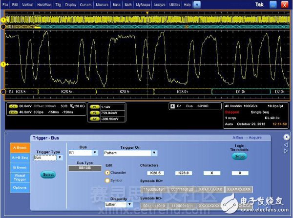
One of the problems with protocol testing is how to do it at 12.5 Gbps. One proposed solution is to use a high speed oscilloscope with a serial data decoder. Many high-end oscilloscopes are now equipped with dedicated trigger chips that trigger 8b/10b data to support JESD204B. Figure 3 shows the serial decoding of the JESD204B data channel at 6 Gb/s, the starting point of the initial channel alignment sequence (ILAS).

Figure 2. Serial decoding of the JESD204B data channel at 6 Gbps and showing the start of the ILAS sequence
Another set of protocol tests can be built around ILAS. ILAS is very complex as a whole, so assigning it to separate components makes protocol testing more meaningful. The following test examples can be used for transmitter measurements to verify their operation. Is the multiframe length correct? Does each multiframe start with the /R/ control code and end with the /A/ control code? Is the /Q/ control code in the correct position? Is the link configuration data and its location correct? ILAS contains data, is it true? How many frames does ILAS last? Is the ILAS on all channels the same? Clearly, protocol testing around ILAS sequences has great potential.
JESD204B doesn't have much handshake, but it can be tested if there is one. Depending on the subclass, a series of tests can be performed. Since the SYNC~ signal can be used as an initial handshake, error reporting, and link reinitialization, do the Tx and Rx components perform the appropriate functions correctly? Does Rx set SYNC~ to start at the correct time and continue for the correct time? Does Tx react correctly based on the duration of the SYNC~ set? Since the data sent over the link also participates in the handshake (such as ILAS), is its content correct and corresponds to the SYNC~ timing?
20 Awg Tinned Copper Wire,Tinned Copper Conductor,Stranded Tinned Copper Wire,Tinned Copper Wire Price
Sowell Electric CO., LTD. , https://www.sowellsolar.com