The MPC860 is a communication controller based on the PowerPC structure. It is not only an integrated microprocessor, but also integrates the functions of many peripherals. The MPC860 has a memory controller with a powerful memory controller that supports a variety of memories, including various new DRAMs and Flash, and seamless interface to memory. It also uses the embedded operating system VxWorks and development environment. Tornado development is very convenient.
In this design, one piece of Intel W28F1283A150 Flash is used as the BootFlash to power up the MPC860. The redundant storage space can completely store the configuration files required by the FPGA. After power-on reset and system startup, the MPC860 processor cooperates with the EPLD to control the download process of the FPGA configuration file and complete the configuration of the FPGA. Using the MPC860, the FPGA can be easily configured, and the FPGA can be remotely configured through the network function of the MPC860, saving the board and the cost of using the dedicated configuration chip. This article describes how to use the MPC860 to configure Xilinx's Virtex II family of FPGAs. The same principles apply to other FPGA chips (including Altera).

In this design, the FPGA adopts Xilinx Virtex-II series è—XC2V4000, and its configuration file download mode has five kinds: master serial mode (master serial), slave serial mode (slave serial), master parallel mode (master select MAP), and Mode (slave selectMAP), JTAG device. Among them, the JTAG mode is used during the development and debugging phase. This design makes the JTAG port directly on the signal processing board, which is convenient for debugging in the development design stage.
Refer to the Xilinx documentation and compare the remaining 4 download modes, which can be divided into serial download mode and parallel download mode. Both the serial download mode and the parallel download mode have two modes: master and slave. The biggest difference between master and slave modes is that the master mode download sync clock (CCLK) is provided by the FPGA; the slave mode download sync clock (CCLK) is provided by an external clock source or an external control signal. The main mode has a much stricter requirement for download timing than the slave mode. Therefore, from the perspective of the processor's easy control of the download process, it is optional to use the slave string mode or the slave mode. This design uses FPGA configuration from serial mode to reduce the resources that occupy the MPC860.
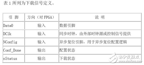
Using MPC860 to configure the FPGA, essentially using MPC860 and EPLD to simulate the download timing of the JTAG interface, complete the download of the FPGA. There are only five valid pins for JTAG, namely nConfig(PROG_B), nStatus(INIT_B), Conf_Done(DONE), DClk(CCLK), and Data0(DIN). nConfig is used to make the FPGA go to the download state. When nStatus, there is no CRC check error. Conf_Done is used to indicate that the download is complete, and DC1k's Data is used to generate the clock and data bits during download. Write 1 bit of data per CD1k clock cycle (the name of the function indicated by the Xilinx FPGA in parentheses).

Pin Direction (for FPGA) Description
Data0 input data pin
DClk input synchronous clock, provided by external clock source or control signal
NConfig input asynchronous reset pin for asynchronous reset configuration logic
Conf_Done output configuration status
nStatus output download status
(1) Start the download sequence to generate a low pulse of more than 2μs on the nConfig pin, waiting for nStatus to respond to a low pulse and Conf_Done. Go low. This time indicates that the FPGA has entered the download state, waiting for at least 5μs to start downloading.
(2) Download Timing The download timing from the string download mode is as shown in FIG.
The data to be downloaded is generated bit by bit on Data0 while the clock is generated on DC1k. Data must be valid for 50ns between the rising edges of the clock, and clocks with both high and low clocks must not be less than 80ns. This process continues until all data downloads are completed. A relatively small amount of wait state can occur during the download without interrupting the download process. If an error occurs, nStatus will be pulled low and the FPGA will exit the operation and must be recalculated in steps 1~3.
(3) End of download After the data is downloaded, it is necessary to continue to provide a number of clocks to the FPGA. The clock should wait at least until Conf_Done goes high.
(4) Start device
Conf_Done is released and pulled high externally.
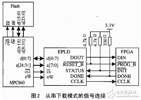
The MPC860 processor controls the signal connection from the string download mode as shown in Figure 2.

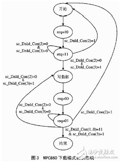
The implementation of the state machine of the MPC860 download mode is done by the PCM860 processor and the EPLD. The MPC860 controls the next state of the state machine by writing Sc_Dnld_Req (1..0), and determines the jump of the flow by judging the contents of the register Sc_Dnld_Con(3..0) in the EPLD.

The state req = "x" in Fig. 3 represents writing data "xx" to the register Sc_Dnld_Req of the EPLD.
Full Range Woofer,Magnet Woofer,Piezo Car Tweeter,Hi-Fi Dome Tweeter
NINGBO BOILINGSOUND ELECTRONICS CO.,LTD , https://www.tweeterspeaker.com