One, MOSFET and other large pads can be punched on the back.
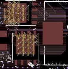
One of the first situations is the need for vias on the pad, for example:
In order to improve the heat dissipation of the MOSFET, we punched the MOSFET pad.

Note: In this case, we need to evenly arrange the hole during the processing of the large pad via hole to ensure that the pad is evenly heated.
Second, some small package resistors and capacitors, do not hit the hole in the pad.
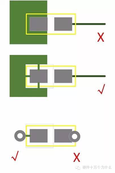
The resistors and capacitors of general labels prevent erection and we need to do windowing.
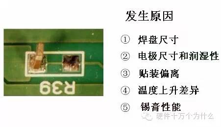
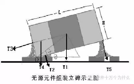
"Tombstoning" phenomenon often occurs in the reflow process of CHIP components (such as chip capacitors and chip resistors). The smaller the component volume, the easier it is to occur. In particular, in the production of 1005 or smaller fishing 0603 SMD components, it is very difficult to eliminate the “tombstone†phenomenon. During the reflow soldering process of the surface mount process, the SMD components will be disorientated due to the soldering defects. As shown in Figure 4, the phenomenon known as "tombstoning" (sometimes called "Manhattan" phenomenon) is vividly described. .
The “tombstone†phenomenon occurs when the solder paste on the pads at both ends of the component is melted at the time of reflow. The surface tension of the two soldering ends of the component is unbalanced, and the end with a larger tension pulls the component and rotates along its bottom. There are also many factors that cause tension imbalance.


So in general, we will do copper-plated pins and open windows to prevent tombstoning. Similarly, we cannot hit holes on the SMT pads to prevent the surface tension of the two pins from being unbalanced.

Can the pad be punched?
Positive point of view: caution;
When designing a PCB board, sometimes the board area is limited or the wiring is more complicated, and the via hole will be considered to hit on the pad of the chip component. The two opinions have been divided into support and opposition. However, in general, it is felt that the method of punching holes in the pads is likely to result in the soldering of the patch components, and should be used as much as possible as a last resort. The two views are briefly described below. Support: Generally, the purpose of punching holes in the pad is to enhance the over-current capability or enhance the heat dissipation. Therefore, the back surface is mainly copper-plated power supply or ground, and few chip components are placed. This prevents leakage of tin during reflow soldering. The problem can be solved by adding green oil to the back of the via hole. The power supply part of the server board that I have contacted is opposed to this: Generally, the SMD component can be used as one of the reflow soldering process or the wave soldering process. Wave soldering requirements pad density should not be too high, the pad is too dense and easy to cause tin short circuit, patch IC pin are more dense, using reflow is the preferred program. And the instrument file can only be used over wave soldering. About wave soldering and reflow soldering can be found on the Internet a lot of introduction. Engineers engaged in PCB design, please understand the production process to know how to design. Protel Fanout rules, is to prohibit the use of holes in the pad . This is forbidden in traditional processes because the solder flows into the vias. There are now two kinds of microvia and plughole processes that allow the vias to be placed on the pads, but are very expensive. Consult the PCB manufacturer. It is best not to punch holes in the PAD and it is easy to cause a false weld. To sort out the layout, the location of a small hole should still be found. However, for patch components, solder reflows through the vias. So use it with caution.
Advantages of punched holes in pads: Convenient routing and avoiding via parasitic inductance.........
Drilled holes in the pad Disadvantages: Over-reflow soldering is easy to form
As long as it solves the problem of reflow soldering, the use of vias in the pad is a good choice for improving the performance of the circuit board based on low cost. Asked some circuit board manufacturers that as long as coated with solder mask on the via hole, and the hole does not open over the general will not form a false weld.
In some companies' products, semi-via holes are made on the BGA pads. After the SMT reflow, the semi-via holes often appear empty or even tin-free.
A semi-via hole is made on the BGA PAD. This process is referred to as blind burial. This hole is called a blind buried hole. If a blind buried hole is used and no electroplating and backfilling is performed, BGA is likely to have problems such as air bubbles and voids during welding.
The biggest advantage of this process is that the coplanarity of the PCB PAD and the PCB also increases the size space of the fine pitch BGA PAD. The disadvantage is that the cost of the PCB is relatively high.
This depends on the manufacturing process, which is now common in some well-manufactured factories. For high-density products, this is called VIP via (Via in Pad). The advantages are: short lead-out distance, space-saving; short outgoing line Small parasitic inductances are good for power integrity and signal integrity; however, if SMT production is not well controlled, it can easily leak tin and cause short circuits.
If space is sufficient, this is generally not recommended. The usual practice is to pull a thick, short wire, and then pull it close to the pad to GND.
Anti-party view: Nothing;
When PCB boards are routed, in the event of high component density, how to route and place vias is indeed a problem. Although many times can solve the problem by reducing the size of the traces and vias and increasing the number of PCB layers, the PCB board cost increases. Here's how to directly place vias on the surface-mount device pads to save space. On the left is the placement of the normal pass hole, which is placed in an empty place with no components. On the right is to place vias on the pads
From the PCB manufacturing process, the vias are placed on the pads and there is no problem in the production process. But the assembly of the circuit board will bring some problems. First of all, because there is a hole in the pad, it will lead to a part of the paste flowing away from the hole after heating, which may lead to "cold solder" or "welding strength is not enough"; in addition, if it is a double-sided chip board, and it happens to be in this Another pad is arranged on the reverse side of the via hole, which may cause the solder paste flowing out to invade the pad and cause a short circuit.
The solution to the above problem is actually very simple, that is, the surface of the via is covered with a solder mask (that is, we usually see the green layer of "oil", mainly green, black, etc.). This is equivalent to "bottoming" the via. Even if the solder paste flows in after the back cover, it will not lose a lot, and it will not flow to the opposite side of the board. In the case of specific operation in the design software, using Altium Designer as an example, double-click the via icon in the PCB window to pop up the via's properties dialog box. Check "force complete tent on top/bottom" to add it to the via. On the solder mask. What you actually see is that the circle map in Top solder or bottom solder is gone, which means that the area will not be exposed.
Here comes the first GEEKVAPE DNA 100C pod mod!
With Geekvape Z100C DNA Kit in hands, the perfect flavor never ends.
DNA 100C Chip, a flavor DIY master with Boost & Replay.
Form-switchable 100W mod with 3A Type-C charging.
New P0.15 XM coils with innovative mesh design, are stronger, more robust, and last 2 times longer than ordinary coils.
greekvape z series vape box,greekvape z series vape mod kit,greekvape z series vape pen,greekvape z series vape device,greekvape z series vape kit
Ningbo Autrends International Trade Co.,Ltd. , https://www.ecigarettevapepods.com