"T", which stands for "Tube", means tubular, and the number after T indicates the diameter of the tube. The T8 has 8 "T" and a "T" is 1/8 inch.
One inch is equal to 25.4 mm. Then every "T" is 25.4÷8=3.175mm
The diameter of the T12 tube is (12/8) × 25.4 = 38.1 mm
The diameter of the T10 tube is (10/8) × 25.4 = 31.8mm
The diameter of the T8 tube is (8/8) × 25.4 = 25.4 mm [T8 is just one inch of the diameter of the tube] (Note: uniform width 39mm, height 52mm)
Commonly used fluorescent lamp length and power: (20w length 620mm; 30w length 926mm; 40w length 1230mm)
The diameter of the T5 tube is (5/8) × 25.4 = 16 mm (Note: uniform width 23.5mm, height 39mm)
Commonly used fluorescent lamp length and power: (8w length 310mm; 14w length 570mm; 21w length 870.5mm; 28w length 1170.5mm; 35w length 1475mm)
The diameter of the T4 tube is (4/8) × 25.4 = 12.7 mm (Note: uniform width 21mm, height 32mm)
Commonly used fluorescent lamp length and power: (8w length 341mm; 12w length 443mm; 16w length 487mm; 20w length 534mm;
22w length 734mm; 24w length 874mm; 26w length 1025mm; 28w length 1172mm)
The diameter of the T3.5 tube is (3.5/8) × 25.4 = 11.1 mm
The diameter of the T2 tube is (2/8) × 25.4 = 6.4 mm
LED fluorescent tubes are manufactured according to the specifications of ordinary fluorescent lamps. The specifications are as large as the same. It is convenient to replace the LED fluorescent lamps with ordinary fluorescent lamps without replacing the brackets to achieve environmental protection and energy saving, which is beneficial to save the cost of replacement.
Cheap 12 Layers PCB stackup and thickness
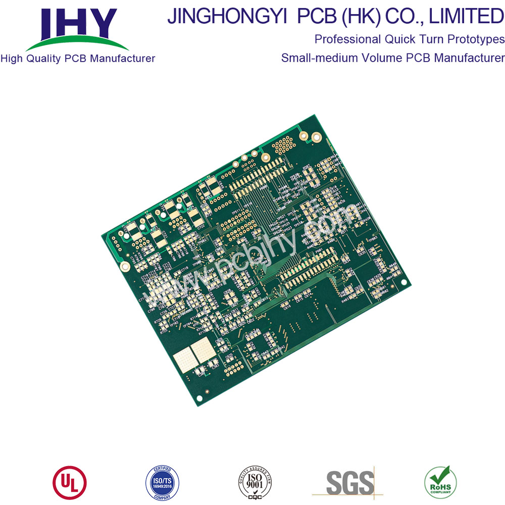
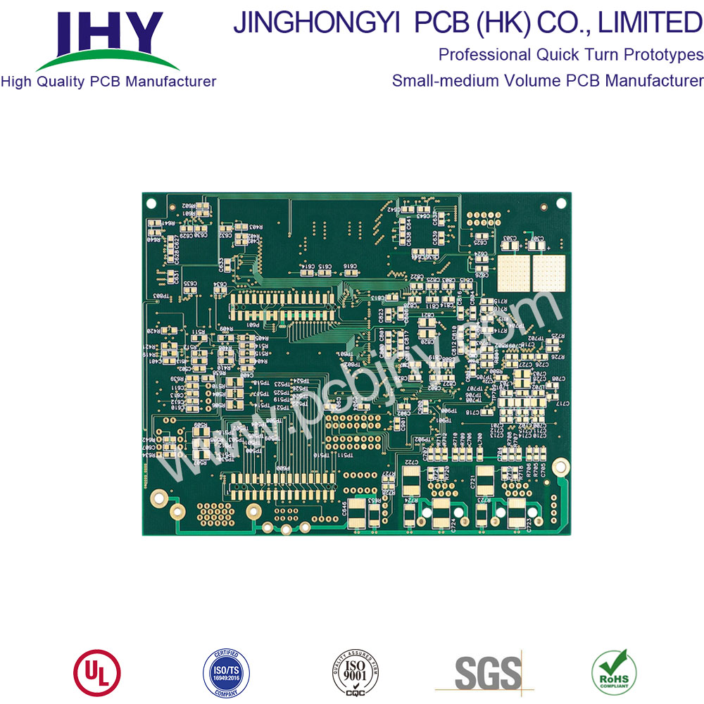
We are one of the few manufacturers in China that can manufacture 12-layer PCB boards on a large scale.
The 12-layer board can usually be manufactured smoothly on a 1.6mm thick FR-4 board. But we've seen more 14- to 16-layer boards are being fabricated into 1.6mm thick boards, but the number of manufacturers that can produce them is limited to manufacturers that can produce HDI boards. Those who can produce HDI boards are increasing.
12 Layers PCB– Heavy industry boards or boards with may tracks
For industrial PC design, 12-layer circuit boards are more popular. Compared with other multi-layer circuit boards, such as four-layer circuit boards, 8-layer circuit boards, 10-layer circuit boards, The price of the 12-layer PCB is still reasonable.

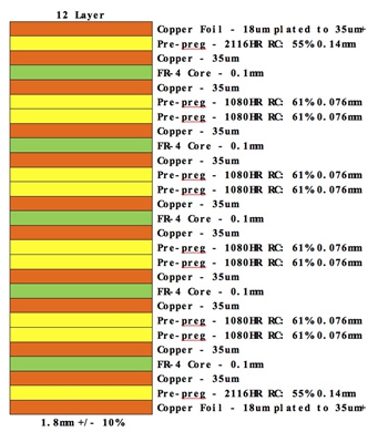
12 Layer PCB stackup and thickness
12 Layer PCB Stack Up
Top Layer †18um Copper Foil (plated to 35um+)
Preâ€Preg †1 x 2116
Layer 2 & 3 †0.13mm Frâ€4 Core with 35um/35um Copper
Preâ€Preg †1 x 2116
Layer 4 & 5 †0.13mm Frâ€4 Core with 35um/35um Copper
Preâ€Preg †1 x 2116
Layer 6 & 7 †0.13mm Frâ€4 Core with 35um/35um Copper
Preâ€Preg †1 x 2116
Layer 8 & 9 †0.13mm Frâ€4 Core with 35um/35um Copper
Preâ€Preg †1 x 2116
Layer 10 & 11 †0.13mm Frâ€4 Core with 35um/35um Copper
Preâ€Preg †1 x 2116
Bottom Layer †18um Copper Foil (plated to 35um+)
Stardand 12 Layer PCB 1.6mm +/†10%

12 layer stackup – 4 GNDs
I use this stackup a lot, provides GND shielding of high speed signals and has tightly coupled Power-Ground planes:
Signal / Solid GND plane / High speed signals and important buses / Solid GND plane / Power / Power or Mixed with signals / Power or Mixed with signals / Power / Solid GND plane / High speed signals and important buses / Solid GND plane / Signal
12 layer stackup – two additional signal layers
Signal / Solid GND plane / Signal / Signal / Solid Power Plane / Power or Mixed with signals / Power or Mixed with signals / Solid Power Plane / Signal / Signal / Solid GND plane / Signal
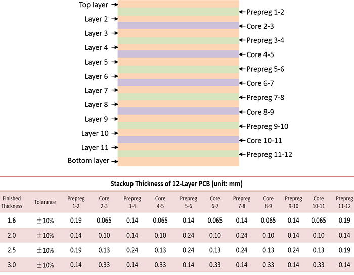
12 layer PCB stackup thickness


12 layer PCB Features and benefits
- Lead-free surface finish and lead-free components
- Long storage time (vacuum and anti-static packaging)
- Improved the speed of signal transmission
- Fast on time delivery
- UL certified and RoHS compliant
- Prototype PCB Manufacturing
12 layer PCB Application
DSL Modem, Solar Battery Charger, Vehicle Tracker, GPS Receiver, Wi Fi Antenna, Bluetooth USB Hub, USB Wireless Router, SMS Modem, Multicoupler Antenna, Phone systems.
12 Layer PCB
Printed Wiring Board,Custom Printed Circuit Board,12 Layer PCB,Custom 12 Layer PCB
JingHongYi PCB (HK) Co., Limited , http://www.pcbjhy.com