According to the theory of voltage control gain circuit and the design principle of amplifier, a variable gain power amplifier monolithic microwave integrated circuit (MMIC) based on GaAs process is designed and fabricated. The schematic and layout simulations were carried out using circuit simulation ADS software, and the influence of the position of the gain control circuit in the amplifier on the performance was studied. Finally, in the frequency range of 6 to 9 GHz, the output power of the 1 dB compression point is greater than 33 dBm. When the control voltage varies between -1 and 0 V, the gain of the amplifier varies between 5 and 40 dB, and the gain control range is reached. 35 dB. The power amplifier and gain control circuit are fabricated on the same monolithic integrated circuit with an area of ​​only 3.5 mm × 2.3 mm. It is flexible, easy to use, high in integration and low in cost, and can be widely used in satellite communication and digital microwave communication. And other fields.
This article refers to the address: http://
Very small aperture terminal (VSAT) and digital microwave communication (also known as P2P communication) systems are commercial microwave wireless information transmission systems with large coverage, high integration, and the same service types and services for all locations. Good characteristics, low expansion cost, short time required, good communication quality and convenient installation.
The power amplifier is the core component of the microwave wireless information transmission system. Its performance directly affects the transmitter's radius of action, linear characteristics and the efficiency of the whole system. It is usually the most expensive component in the system. The trend of miniaturization of contemporary microwave wireless information transmission systems is becoming more and more obvious, which requires higher integration of components.
Foreign commercial monolithic power amplifiers have been researched abroad. Among them, Japan's Eudyna has better product performance and the largest market share. The US company Hittite and Triquint have also launched corresponding products in the past two years. China has also actively carried out related research work on GaAs material growth and device development.
Since the power amplifier is applied in the commercial field, it has high requirements on its performance and cost. In this paper, the function of the conventional power amplifier is expanded by the circuit design, and the gain control function is added, which can realize the miniaturization of the system. Reduce costs, while not affecting the power amplifier's output power and efficiency and other related indicators.
In this paper, the GaAs high electron mobility transistor (PHEMT) process, which is a mature microwave monolithic integrated circuit, is used to develop a multi-function power amplifier. The process is stable and the yield is high, which is irreplaceable in shortening the development cycle and reducing the cost. status. The area of ​​the multi-function power amplifier monolithic integrated circuit developed in this paper is the same as the power amplifier area of ​​the same index, which is about 8 mm2. The area of ​​the voltage-controlled variable attenuator (VVA) of the traditional outdoor unit is about 1.7 mm2. The multi-function power amplifier saves the chip area by 17.5%, which is beneficial to system miniaturization and cost reduction.
1 design principle of gain control circuit
The function of the gain control circuit is to change the gain of the amplifier by changing the control voltage. The position of the gain control circuit in the amplifier is very important. If it is placed at the final stage of the amplifier, it will affect the output power due to its own loss. If it is placed in the middle, the intermediate stage of the amplifier will not be able to saturate the final stage, thus affecting effectiveness. Through the above analysis, the gain control circuit is placed in the first stage of the amplifier.
The principle of the gain control circuit is shown in Fig. 1. It consists of two field effect transistors. The drain of FET1 is connected to the source of FET2, and the RF signal is input from the gate of FET1 and from the drain of FET2. In Figure 1: Vc is the control voltage; Vgs is the gate voltage; Vdd is the drain voltage; V1 is the voltage at the junction of the two FETs; Ids is the drain-to-source current of FET1 and FET2, the source of FET1 in Figure 1. The drain of FET2 is connected to the same node, so Ids flows through FET1 and FET2 at the same time. The circuit changes the gain by changing the voltage value of Vc.
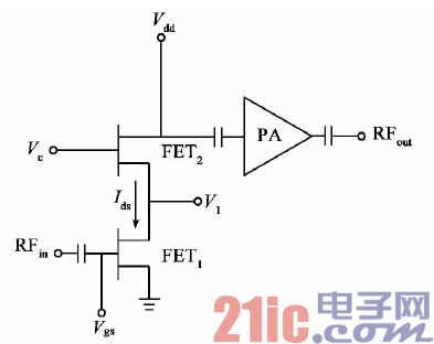
Figure 1 Gain control circuit topology diagram Transconductance gm when the FET operates in the saturation region, the relationship between Ids and Vgs is shown in Figure 2. When the gate voltage Vgs of the FET 1 remains unchanged, the source-drain resistance value does not change greatly, and the impedance at the operating point is about 10 Ω. It is known from Ohm's law that the voltage value of V1 is determined by Ids. The drain voltage Vds of FET2 remains unchanged. When Vc changes, the gate voltage of FET2 changes accordingly. As can be seen from the graph of Fig. 2, when the gate voltage changes, gm changes, and the amplification factor of FET2 changes accordingly. At the same time, when the gate voltage of FET 2 changes, according to FIG. 3, Ids will have a large change. According to the previous analysis, when Ids changes, the value of V1 will also change accordingly. When V1 is less than 1V, FET1 operates in the linear region of Figure 3, and the gain is greatly affected by the leakage voltage, so when V1 changes The magnification of FET1 will also change accordingly. Thus, the gains of both FET1 and FET2 are controlled by Vc, and the common gain variation amount becomes the gain variation range of the power amplifier.
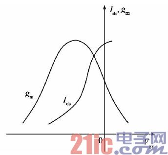
Figure 2 gm, Ids vs. Vgs
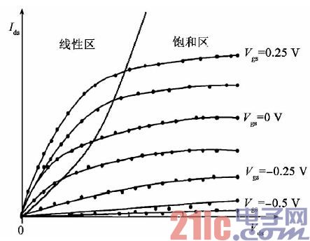
Figure 3 Vds, Vgs and Ids curve
2 Power amplifier design principle
In this paper, the design of the power amplifier is carried out using the model of the GaAs PHEMT process line of the 13th Research Institute of China Electronics Technology Group Co., Ltd. The output power of the GaAs PHEMT FET has a total output of 0.6 W, and if it needs to output 33 dBm, that is, 2 W power, The total gate width of the final stage is 4mm, using 4 power units, and the total grid width of each unit is 1 mm. To get a high-efficiency power amplifier, you need to carefully consider the total gate-to-width ratio of each stage of the FET to achieve maximum efficiency.
According to the design goal, the corresponding circuit topology is determined. The choice of topology determines the performance of the whole circuit. The load is pulled on the active device to find out the input and output impedance of the active device when it can output the maximum power on the impedance chart. position. The 1 mm gate width model used in this paper is shown in Figure 4. Figure 4(a) shows the model plate for device modeling and Figure 4(b) shows the large signal model fitted by measurement parameters. The design of the output matching network looks at the maximum power output, and the topology is shown in Figure 5.
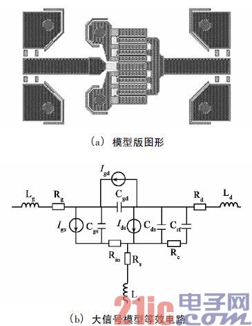
Figure 4 1 mm gate width device model
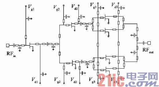
Figure 5 Power amplifier topology 3 CAD design simulation and test results
According to the topology of Figure 1 and Figure 5, the circuit is designed and optimized using the ADS simulation tool in combination with the GaAs PHEMT process model.
The ADS is used to design and optimize the passive components of the power amplifier monolithic integrated circuit, adjust the size of matching components such as capacitors and strip lines, and optimize the parameters such as the working frequency band, gain, standing wave, output power and efficiency of the circuit. The large-signal simulation is performed by the harmonic balance simulation software in ADS, and the electromagnetic field simulation is performed on the layout. ADS simulation includes schematic simulation and layout simulation. In the schematic simulation, the initial values ​​of the various components of the circuit are obtained and optimized according to the design goals, but the schematic simulation only considers the independent testing of active devices, metal strips and other devices. The model does not consider the mutual coupling between the devices in the layout, and the obtained component values ​​are different from the actual situation. In order to simplify the area of ​​the integrated circuit, the device spacing is close to the single line spacing, the influence of the line coupling on the performance of the amplifier must be considered. Therefore, using the 2.5D layout simulation tool MOMENTUM, the inter-line coupling and interlayer between the circuits are performed by the method of moments. The coupling was performed by electromagnetic field simulation.
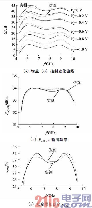
Figure 6 Simulation and test results of the power amplifier
The dotted line in Figure 6 is the simulated version of the electromagnetic field simulation results after optimization, and the solid line is the test result. It can be seen from the figure that the gain control range is 35 dB, and the output power Po (1 dB) of the 1 dB compression point is greater than 33 dBm in the frequency band, and the power added efficiency ηPAE is greater than 30%. The power amplifier monolithic integrated circuit with gain control function designed in this paper uses GaAs process for chip verification and carrier test. The installation of monolithic integrated circuit adopts mounting and bonding process. The installed carrier is shown in Figure 7. . Analyze the simulation and the measured results. The gain curve has a good agreement with Vc of 0, -0.2, -0.4 and -0.6V. There is a certain deviation when Vc is -0.8V and -1V. The measured gain is lower than the simulation. 2~4dB, the reason may be that when the gate voltage of the FET is biased at -0.8V and -1V, it is close to the pinch-off region, and the fitting accuracy of the model transconductance is poor. The transconductance model under the bias is actually used. The fitted value is lower. The measured curve of the 1dB compression point output power and the power added efficiency agree well with the simulation curve. Both indexes are tested at Vc=-0.6V. At this time, the amplifier works in the saturation region, and the model fitting value is The area is closer to the actual value, so the two indicators agree well with the simulation results.
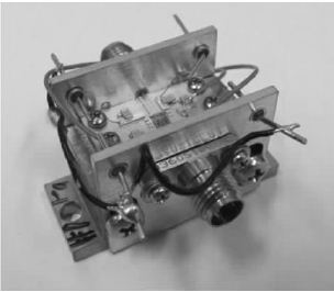
Figure 7 carrier installation completion map
4 Conclusion
In the design of monolithic integrated circuit power amplifier with gain control function, this paper analyzes the principle of gain control circuit and the influence of gain control on the power amplifier index. Using electromagnetic field simulation tool, the layout area is reduced on the basis of ensuring circuit performance, which greatly reduces The cost of monolithic integrated circuits; verifying the correctness and feasibility of the monolithic integrated circuit design method and ideas through tape and test; adding gain control without increasing the area of ​​the power amplifier monolithic integrated circuit and reducing the performance Function, reduced cost, and broad application prospects in the fields of satellite communication and digital microwave communication.
M12 Connection Cable provides a wide range of metric for small Sensors and actuators. The connector system provides a future-proof interface that supports higher-bandwidth needs, meeting the requirements of up to 10GB/s. Connectors are either factory TPU over-molded or panel receptacles supplied with sold-cup for wire connecting or with PCB panel solder contacts. Field attachable / mountable Connector is also available for your choice.
M12 connection cable,M12 3 pin connection cable,M12 4 pin connection cable,M12 5 pin connector cable,M12 8 pin connector cable
Kunshan SVL Electric Co.,Ltd , https://www.svlelectric.com