introduction
With the extensive promotion and application of modern high-tech, the urban traffic signal control system presents two major development trends:
(1) changes in the control concept;
(2) Application of artificial intelligence technology.
The intelligent traffic signal control machine is mainly used in those places where the traffic volume at the intersection of the city is large, the traffic flow conflicts and complex intersections and ramps, and the traffic flow direction on some road sections to improve the traffic environment. The purpose of managing and diverting traffic is to adjust, control and guide traffic flow on the road through traffic signals to maintain traffic order, ensure safe traffic and reduce traffic accidents.
1 Traffic Signal Control System Overview The intelligent traffic controller is the executive of the traffic control algorithm. The controller host hardware adopts a modular design that can be tailored. The software is written in C language with good portability. The main function is to realize the automatic control of intersection traffic lights with the single chip as the core. The main functions are automatic multi-time timing control. Semi-automatic control, manual commutation, additional left turn green light, sidewalk traffic lights, etc.
2 Traffic signal controller hardware design
2.1 The traffic signal hardware as a whole can be seen from the hardware overall frame diagram of the traffic signal machine shown in Figure 1 and Figure 2 and the core circuit overall framework. The core circuit board is mainly based on single-chip microcomputer, including clock module and storage module. , keyboard input module, anti-crash module, scheme control display circuit module, lamp color display circuit module, time display module. The above modules are briefly described below.
This article refers to the address: http://
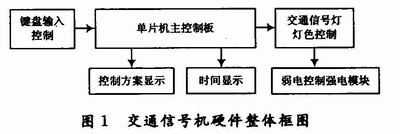
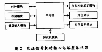
(1) Clock module: The DS12887 chip is used to communicate with the single-chip AT89C51 to realize real-time time clock information reading.
(2) Memory module: The 93C46 chip is used as the external memory of the microcontroller to store the time table information.
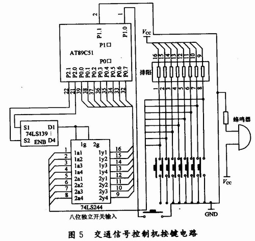
(3) Keyboard input module: Design the keyboard input circuit with 74LS244.
(4) Anti-crash module: Use 74LSl23 to form a reset circuit to prevent the MCU from entering an infinite loop.
2.2 Clock module circuit design The main task of the clock circuit is to use the communication between the clock chip and the microcontroller to enable the microcontroller to obtain standard real-time clock information. Here, we choose the DSl2887 clock chip, which has its own battery and can store the clock information when it is powered off.
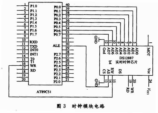
The clock module circuit is shown in Figure 3.
(1) When the chip select segment CS (13 pin) of the clock chip is active low, the MCU can read and write it;
(2) RD (P3.7, 17 pin) of the single chip sends a read data request to the RD (DS, 17 pin) of the clock chip. This port effectively indicates that the MCU is reading the clock data.
(3) WR (P3.6, 16 pin) of the single chip sends a write request to the WR (15 pin) of the clock chip. This port effectively indicates that the MCU is writing data to the clock chip.
(4) The ALE (30 pin) of the MCU is used to access the clock chip (AS, 14 pins) and output pulses to latch the lower 8-bit address;
(5) The clock Rester (18 pins) is connected to the Vcc in series with a 100 kΩ resistor, and the other line is directly connected to Vcc;
(6) The P0 port of the MCU communicates with the AD port of the clock chip to obtain real-time clock information.
2.3 Memory Module When designing the circuit, in order to use the I/O port of the MCU with higher efficiency, the serial flash memory 93C46 chip is used to design the memory module circuit.
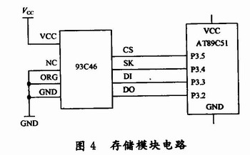
It can be seen from the memory module circuit of Figure 4 that the single-chip AT89C51 uses the P3.5 port to make the chip select signal of the 93C46 chip valid, the clock communication through the P3.4 port, and the data transmission using P3.3 and P3.2. Realize the storage of the information of the timesheet.
2.4 Key circuit design The panel design requires a total of 9 buttons. It uses the time division multiplexing of the P0 port of the single chip microcomputer to solve the connection between 8 buttons and the single chip microcomputer. The remaining one button is connected to the P1 port separately. The 74LS244 chip and the 74LS139 chip are used in the circuit design, and the wiring diagram is shown in Figure 5.
2.5 traffic light display module as shown in Figure 6 of the traffic light display circuit, the control chip used is basically the same as the time display module, using a 74LS139, two 74LS273; the circuit is still used to output data through the P0 port of the microcontroller Control the lighting of the traffic lights, use the 74LSl39 chip to achieve different phase traffic light control data output at different times.
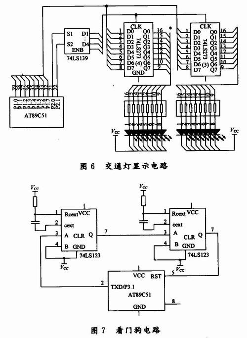
2.6 Anti-Crash Circuit In the traffic signal control system, in order to prevent the "dead" phenomenon, the system has an automatic recovery capability, in which the anti-crash system, the so-called "watchdog", is set up. The basic wiring diagram is shown in Figure 7. Show.
3 Conclusions and prospects A hardware design method for a new traffic signal control system is proposed. According to the development of traffic signals in modern cities, and the requirements of the overall hardware of traffic signals, various parts of traffic signals are given. The hardware is configured to meet the needs of urban traffic signal control.
With the development of technology and the increasing amount of social traffic, the hardware part of the traffic signal system can be upgraded and expanded to meet the needs of higher traffic control.
S-yuan Electronic Technology Limited , https://www.syuanelectronic.com