Design of Ultra Low Intermediate Frequency CMOS Down Mixer
The low-IF architecture is widely used in the design of receivers due to its strong image suppression capability and ease of integration. As one of the important modules of the receiver, the mixer's main function is to complete frequency conversion, and its performance has a great influence on the receiver. An ultra-low intermediate frequency CMOS mixer working in the GSM 850 frequency band is designed. In order to improve conversion gain and reduce noise, a shunt unit is added to the input stage. Apply common-mode feedback at the output stage to stabilize the output level. The frequency band where the mixer works is 869-894 MHz, and the intermediate frequency output is 100 kHz. The simulation results show that the gain is 17 dB, the third-order intermodulation point is 9.6 dB, and the noise figure is 17.5 dB.
Keywords: ultra-low intermediate frequency; CMOS; downmixer; Girlbert
With the rapid development of wireless communication, people have put higher and higher requirements on wireless communication transceivers. Receivers with low-IF architectures are widely used due to many advantages such as high integration and strong image rejection. As one of the important modules of the receiver, the mixer's main function is to complete frequency conversion, and its performance has a great influence on the receiver. This paper uses TSMC 0.18μm CMOS technology to implement a down-mixer applied in the GSM band (869 ~ 894 MHz). The structure of the mixer is a Gilbert double-balanced structure, and the output is an ultra-low intermediate frequency of 100 kHz. Good design results.
1 Main circuit design Figure 1 is a typical Gilbert unit. In the figure, the differential tubes M1 and M2 are the transconductance stages of the mixer, and M3, M4, M5, and M6 are the switching stages of the mixer. The radio frequency signal is input by the grids of M1 and M2 tubes, the local oscillator signal is input by the grid levels of M3, M4, M5, and M6, and the intermediate frequency signal is output by the drain level of the switch tube. When the local oscillator signal is strong enough, the current output by the mixer is:

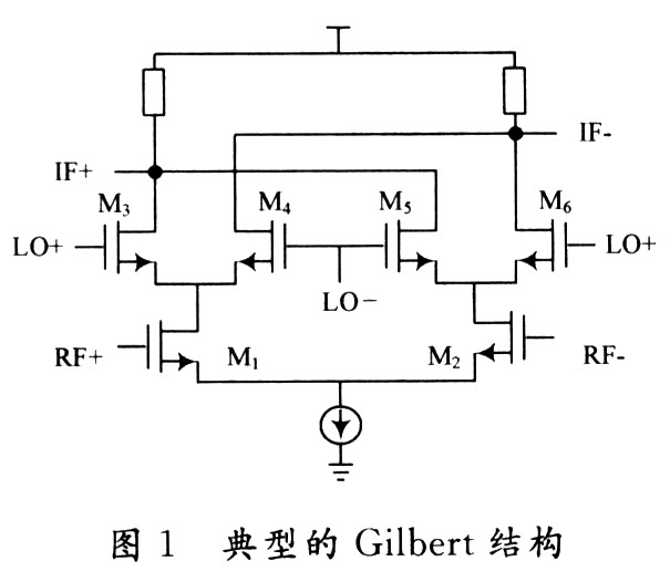
This current is converted into the required voltage signal after passing through the output load. Based on the simple Gilbert structure, in order to achieve the required performance, the circuit has been improved as follows. The specific circuit design is shown in Figure 2.
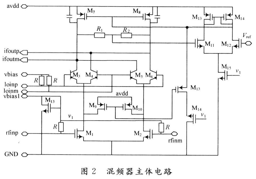
1.1 Design of the driver stage The tail current source is removed in the driver stage, and the current mirror structure is used to bias the M1 and M2 tubes. The advantage of this is that it can improve the linearity of the circuit and increase the output voltage margin. Although the tailless current source structure may allow more substrate noise to enter the signal path, the careful layout design can well reduce the influence of the substrate. The linearity of the mixer is proportional to the magnitude of the bias current of the driver stage and the overdrive voltage. The greater the bias current, the greater the overdrive voltage and the better the linearity. According to the gain formula of the mixer ![]() High gain requires large load resistance. Excessive bias current will make the voltage drop on RL too large, causing the switch pair and the drive tube to deviate from the saturation region, and will increase the noise of the switch pair and increase power consumption. Therefore, the current extraction circuit composed of M9, M10, M13 and M14 is adopted. The current drawn cannot be too large, otherwise it will seriously affect the linearity of the mixer. The Vgs of the M1 tube are provided by the M13 tube, according to:
High gain requires large load resistance. Excessive bias current will make the voltage drop on RL too large, causing the switch pair and the drive tube to deviate from the saturation region, and will increase the noise of the switch pair and increase power consumption. Therefore, the current extraction circuit composed of M9, M10, M13 and M14 is adopted. The current drawn cannot be too large, otherwise it will seriously affect the linearity of the mixer. The Vgs of the M1 tube are provided by the M13 tube, according to:

The value of Vgs can be determined by adjusting the input reference current source under a certain aspect ratio. The channel lengths of M1 and M3 are both 350 nm, and the ratio of the width of the two tubes can be adjusted to control the magnitude of the bias current of the M1 tube. The current flowing through M1 in the design is 1.2 mA, and the current value drawn is about 0.5 mA.
1.2 The design of the switch tube The design consideration of the switch tube is mainly the influence of the flicker noise of the tube. The channel bandwidth of GSM is 200 kHz, and the intermediate frequency of 100 kHz can make the frequency of the local oscillator signal exactly in the middle of the center frequency of the two channels, avoiding the interference of the local oscillator signal on the signal in the channel. The 100 kHz IF signal requires extremely low flicker noise corners, which are required to be within 20 kHz in the design. According to the formula of the flicker noise corner:
![]()
To reduce the corner frequency can only increase the device area (the value of WL). For CMOS transistors, the flicker noise corner generally falls in the vicinity of 500 kHz to 1 MHz, which is far from meeting the design requirements. So the switch tube is designed with 4 Bipolar parasitic tubes to replace the switch stage composed of MOS tubes. This can make the flicker noise corner within 20 kHz.
1.3 Design of output stage The output stage adopts PMos current mirror as the load, and the function of two MIM capacitors connected in parallel with M7 and M8 is to filter out higher harmonics. The area of ​​M7 and VIs tubes must be as large as possible in order to effectively reduce flicker noise. In the design, M and M8 tubes take the value W / L 320μm / 1μm. Since the DC bias level of the output stage cannot be determined, common mode feedback must be added. This task is accomplished by a simple op amp composed of M ... M12, M13, M14. The value of Vref is 2.1 V. The common-mode level taken out by the resistor is compared with Vref. The output level is fed back to the gate of M7 and M8 from the drain of M14 to achieve the purpose of controlling the output level.
2 Simulation results Figure 3 is the simulation results of the circuit gain, reaching about 18 dB at 880 MHz.
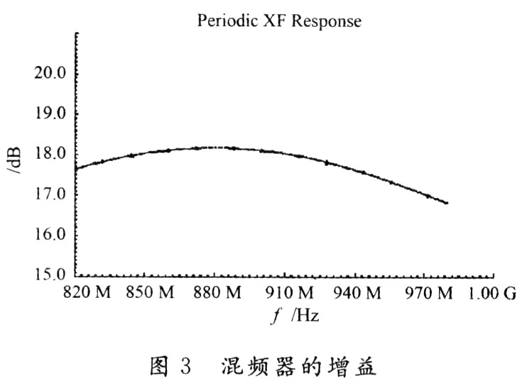
Figure 4 is a simulation of the noise figure. The flicker noise inflection point is around 20 kHz, and the noise reaches 17.5 dB at 100 kHz.
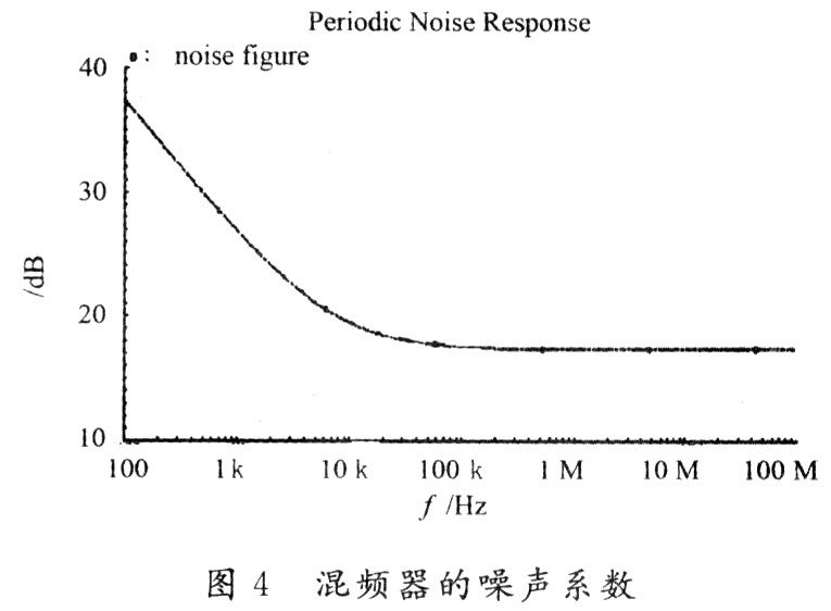
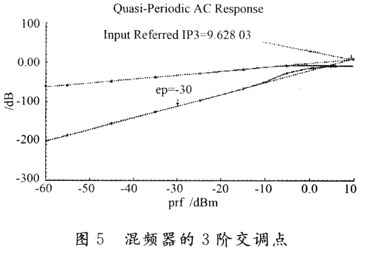
Figure 5 is the test of the third-order intermodulation point. When the local oscillator signal is -5 dB and the input RF signal is -30 dB, the value of the third-order intermodulation point is 9.6 dB.
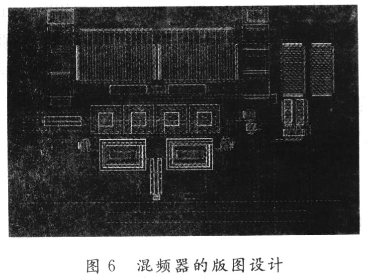
3 layout design Figure 6 is the layout of the design. It should be noted that the traces of high-frequency differential signals should be as symmetrical as possible.
4 Conclusion This article has designed an ultra-low intermediate frequency mixer working in the GSM band, using TSMC 0.18μm CMOS process, the output intermediate frequency is 100 kHz, the gain is 18 dB, the noise figure is 17.5 dB, the third-order intermodulation point It is 9.6 dB and can be used in GSM receivers.
Our company specializes in the production and sales of all kinds of terminals, copper terminals, nose wire ears, cold pressed terminals, copper joints, but also according to customer requirements for customization and production, our raw materials are produced and sold by ourselves, we have their own raw materials processing plant, high purity T2 copper, quality and quantity, come to me to order it!
Cable Terminals
Taixing Longyi Terminals Co.,Ltd. , https://www.lycopperlugs.com