Although image sensors based on CMOS technology have been widely used in many applications, some demanding industrial imaging applications still require the unique performance of CCD image sensors.
As an example, the key flat panel display production line terminal inspection is still mainly performed by cameras using CCDs, because they can provide high resolution and excellent image uniformity, which is currently not available in CMOS image sensor technology.
This type of detection is usually performed by a camera based on ON Semiconductor's 29 million pixel (Mp), 35 mm optical format KAI-29050 image sensor and other devices. However, the resolution of flat panel displays is getting higher and higher, and the resolution of cameras used to detect them also needs to be improved accordingly. To meet this demand and retain the standard 35 mm optical format, a new pixel design that can reduce the pixel size while retaining the key performance and image uniformity specifications required by the application is required.
Demand for high-performance, high-resolution imaging
Today, imaging drives the productivity benefits of industrial applications, from traffic monitoring, license plate recognition, to barcode scanning, robot guidance, machine vision, and more. Although each application has its own unique requirements (some require a high frame rate, others require a wide dynamic range, low light sensitivity, or a different key parameter), some applications mainly require the highest level of image detail, requiring development with very High-resolution image sensor.
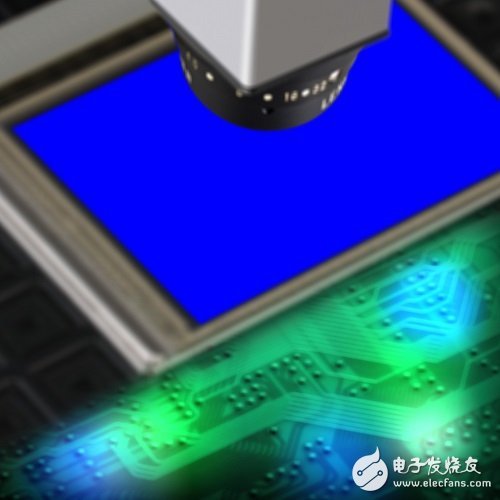
A good example is the terminal inspection of the flat panel display production line. This process is to confirm that the three sub-elements of red, green and blue in each display pixel can work normally. As the application of displays continues to expand in more fields such as mobile devices, tablets, televisions, vehicles, monitors, and more, the resolution of these displays is also constantly improving, from 1080p to 4k/Ultra HD and even higher. This places unique requirements on the cameras used to monitor these displays during the manufacturing process. It needs to provide the details needed to be able to resolve the additional pixels and substructures present in the display without sacrificing the image quality and uniformity required for the application .

Figure 1: Using a camera to detect flat panel displays
Other examples of high-resolution imaging include high-end surveillance (acquisition of a wide field of view image with a resolution sufficient to magnify any position) and aerial photography (higher resolution can provide additional imaging details, or allow aircraft to fly higher And reduce the number of flights). But in all these examples, the application requires not only very high resolution, but also very high image quality, which can be measured by specifications such as image uniformity, noise, and dynamic range.
In view of this comprehensive demand, this application has been relying on the image sensor based on Interline Transfer CCD (ITCCD) technology, even if it is expanded to a large optical format, it can retain the key imaging performance parameters. This technology can capture images with very high image uniformity, and a true global shutter design can capture moving scenes without introducing imaging artifacts. In addition, this technology can provide a wide exposure range and low dark current, and can achieve image exposure in the range from a few microseconds to one second or longer.
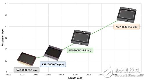
Interline Transfer CCD technology has been used in the development of high-resolution, large-format image sensors for more than 15 years, and its resolution has been gradually improved with market needs. For example, the KAI-11000 image sensor in 2003 provided a resolution of 11 million pixels in a 35 mm optical format; but by 2011, this same optical format could support almost three times the resolution.

Figure 2: Improvement of ITCCD resolution in 35 mm optical format
This advancement in increasing resolution while preserving the optical format is very important to achieve simplified field upgrades for cameras used in these applications, because when deploying higher resolution cameras, neither the placement of the camera nor the lens need to be changed.
Strict requirements bring major design challenges
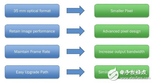
In order to continue to increase the resolution of devices (such as KAI-29050) from the existing 29 million pixels while retaining the 35 mm optical format, a smaller pixel format is required to place more pixels in a given area . However, in order to retain the key imaging parameters in this smaller pixel at the same time, such as image uniformity, dynamic range, and noise floor, in addition to simply reducing the size, it is also necessary to improve the pixel design.

Figure 3: Design challenges
As the number of pixels in a device increases, unless the output bandwidth of the device can be increased, the overall frame rate will decrease (this may also be required for some applications). Maintaining backward compatibility with current sensors and cameras is essential to help camera manufacturers and end customers simplify the upgrade path required to support and adopt new devices.
35mm optical format high-performance ITCCD sensor
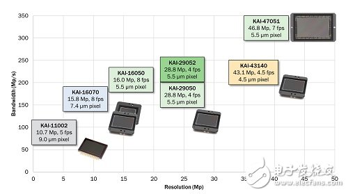
ON Semiconductor’s KAI-43140 image sensor provides an example of how to meet these design challenges, using the 35mm format to provide a higher resolution for demanding applications. The new device uses brand new 4.5μm ITCCD pixels and provides 43 million pixels in a 35 mm optical format. Compared with the widely used 29 million pixel KAI-29050, the resolution has increased by 50%. However, even with this smaller pixel size, the key imaging performance levels are still retained (including high smear suppression and linear dynamic range exceeding 60dB), and through the use of advanced process design, the uniformity of the entire category is eliminated Artifacts, image uniformity is actually improved.
The updated output amplifier can increase the bandwidth of the 4-tap device by 50%, and despite the increased resolution, it can still provide the same final frame rate as the 29-megapixel device. Since KAI-43140 is still based on ITCCD technology, it retains features such as electronic shutter and extensive exposure support, which are the hallmarks of this technology.
Importantly, KAI-43140 uses the same package as KAI-29050, allowing current camera designs to support new devices with only minor electrical changes. This greatly reduces the design risk for camera manufacturers and enables them to bring cameras with higher resolution and performance to the market faster and at a lower cost.
to sum up
The development of imaging sensors that meet the stringent requirements of advanced industrial applications requires far more than simply "pull" more pixels into a smaller package. By adopting advanced pixel design, higher resolution can be provided at a given optical node without sacrificing the required performance.

Figure 4: ON Semiconductor's large format ITCCD image sensor
However, even with these improvements, it is important to realize that the "latest" imaging device is not necessarily the "best" device for all applications (even for applications that require very high resolution). Not only have different options for resolution, but also different options for parameters such as light sensitivity, dynamic range, frame rate, and even price, are critical to determining the most suitable image sensor (and imaging technology) for a given application . This highlights the importance of having a broad lineup of devices (even if it is focused on a specific set of applications, such as requiring very high resolution), and emphasizes the need for continuous development of new products using technologies such as Interline Transfer CCD.
Shenzhen Hongyian Electronics Co., Ltd. , https://www.hongyiancon.com