As the market's demand for feature-rich mobile phones becomes stronger and stronger, analog switches with special application performance have been continuously favored by the final design. This will not only reduce the cost of materials (BOM), but also help improve design performance and meet the time-to-market requirements. This article will guide system designers through a number of practical use cases on how to reduce pop noise, detect chargers, and improve eye opening.
At the same time, this article also illustrates the benefits of using this high-performance analog product in the development of the mobile phone market to multimedia design by comparing traditional solutions with integrated solutions.
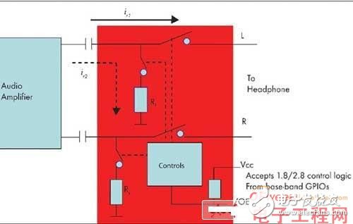
Reduce impact noiseThe impact noise caused by inrush current is still a daunting challenge for designers, especially when the end user initiates the switch between music and call functions. As long as the end user turns on the music function, this annoying noise will give people an unpleasant experience. As shown in Figure 1, when the audio amplifier is working, the power on/off surge current through the AC coupling capacitor is the culprit for the impact noise, and the audio common-mode voltage will rise sharply at this time.
There are multiple solutions currently on the market. One of them is to add an additional amplifier to make the audio output have a "0V" bias, thereby minimizing the size of the AC coupling capacitor immediately before the headphones. Because most headphone amplifiers are integrated into the baseband processor or power management unit (PMU), adding this amplifier not only increases the material cost, but also increases the power consumption.
Figure 1 shows another method that adds an independent charging path to the audio signal path, allowing the AC coupling capacitor to be fully charged before being switched to the earphone or main path. This can be controlled by the general-purpose I/O of the baseband processor, so that the audio amplifier and switch are powered on first, and the main channel switch is in the off state at this time. The common mode voltage of the audio output will start to rise from 0 to VCC/2. After a period of time (with 10ms as a reference), the two ends of the coupling capacitor are charged to the same potential, and then the main channel will be turned on and there will be no surge current , Because at this time the voltage difference between the two poles of the capacitor is 0V.

â–² Figure 1: Audio switch with low THD and negative swing function can eliminate audio impact noise.
This switch is very suitable for mobile phones and MP3/MP4 players with a single USB connector (D+/D- pin) shared by the headset and USB data cable. Low total harmonic distortion (THD) is very important for audio channels. In addition, because the switch is placed after the AC coupling capacitor, it must handle the large reverse signal swing at low THD. The ultra-low turn-off capacitance of this switch allows high-speed USB signals to be "wired-ORed" with the device. The lower parasitic capacitance is also the key to the compliance test of the high-speed USB 2.0 standard.
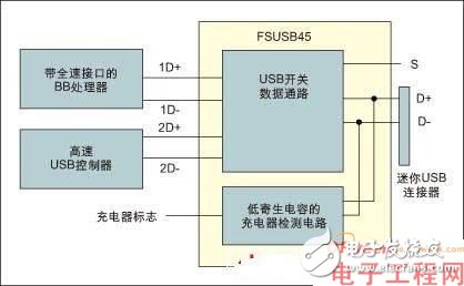
Special application USB switchWith the current market trend shifting to a single USB charger/data port, USB switches for special applications have become a conventional configuration in the design of mobile phones with charger detection functions. Figure 2 is an example of such a switch application.

â–² Figure 2: The USB switch with charger detection function is very suitable for high-speed USB applications, and its USB power and data ports are shared.
For two main reasons, a switch with low on-capacitance is required in this design. First, since the baseband processor and high-speed USB controller output share the same D+/D- pins on the connector side, when the mobile phone enters high-speed USB 2.0 mode (such as music download or flash memory function), the baseband USB1.1/ 2.0 The output capacitor of the full-speed controller. Any extra capacitance on the D+/D- lines will damage the eye opening of the high-speed USB signal. Secondly, in the high-speed USB mode, the extra traces suspended on the D+/D- lines must be cut to effectively avoid signal reflections caused by the fast rising/falling edges of the 480Mbps USB signal.
Since a single USB port needs to be used for both the charger and the data function at the same time, the charger detection function has been very popular in the current design. The traditional solution is to feed the D+/D- line to the internal A/D converter to determine whether the D+/D- line is short-circuited. As mentioned earlier, the main limitation of this solution is that the high input capacitance of the GPIO port of the baseband processor will add additional capacitive reactance to the data line. This newly added capacitive reactance will greatly affect the effective triggering of signals at high data rates. Adverse effects, and this indicator is part of the USB 2.0 conformance test (for example, 480 Mbps for USB 2.0 signals). Of course, another disadvantage of this method is that it also occupies the resources of the system A/D converter.
In these applications, in order to realize the isolation between the charger detection and the output capacitance of the full-speed USB controller, a USB switch with an ultra-low internal capacitance detection circuit is required. At the same time, the USB channel selection pin (S pin in Figure 2) used to determine which USB channel is selected as the output must be able to recognize 1.8 V and 3 V logic inputs (note: 1.8 V and 3 V in the baseband processor GPIO output Are quite commonly used).
The traditional switch selection pin can accept input "high" (Vih) level up to 2.0 V (TTL logic). When the switching power supply (VCC) is directly taken from the battery, this level can cause serious leakage current. With the ability to recognize 1.8 V input logic levels, external level conversion devices can also be eliminated, allowing designers to further reduce material costs. For example, ICs such as Fairchild’s FSUSB45 have ultra-low on-capacitance (7pF), small size (1.4×1.8 mm), charger detection function and 1.8 V control logic identification, etc., which can well meet USB data path switching. Design needs.
Summary of this articleAnalog switch applications have been developing from pure audio switch functions to more advanced products. These advanced products can simultaneously provide value-added design features and powerful I/O-to-ground ESD capabilities. With the popularization of multimedia features such as MP3/MP4 players and GPS/WiFi functions in final applications, designers need more special switches that can not only provide low-distortion switching channels, but also solve standard compliance tests. The design challenges faced. In addition, these switches can reduce material costs and significantly shorten the time to market.
Pc Material,Pc Plastic Material,Pc Clear Material,Pc Material Properties
WENZHOU TENGCAI ELECTRIC CO.,LTD , https://www.tengcaielectric.com