As mentioned earlier, FPGA is a product of further development on the basis of programmable devices such as PAL, GAL, EPLD, and CPLD. It emerged as a kind of semi-custom circuit in the ASIC field, which not only solves the deficiencies of custom circuits, but also overcomes the shortcomings of the limited gate circuits of the original programmable devices.
Because FPGA needs to be programmed repeatedly, its basic structure for realizing combinational logic cannot be completed by a fixed NAND gate like ASIC, but can only adopt a structure that is easy to repeatedly configure. The look-up table can meet this requirement well. At present, mainstream FPGAs all use the look-up table structure based on SRAM technology, and some military and aerospace-grade FPGAs use the look-up table structure of Flash or fuse and anti-fuse technology. The method of changing the content of the look-up table by programming the file can realize the repeated configuration of the FPGA.
According to the basic knowledge of digital circuits, for an n-input logical operation, whether it is an AND OR operation or an exclusive OR operation, there can only be at most 2n kinds of results. Therefore, if the corresponding result is stored in a storage unit in advance, it is equivalent to the realization of the function of the NAND gate circuit. The principle of FPGA is also the same. It configures the content of the lookup table by programming a file, thereby realizing different logic functions in the same circuit.
Look-up table (Look-Up-Table) is abbreviated as LUT, which is essentially a RAM. Currently, 4-input LUTs are mostly used in FPGAs, so each LUT can be regarded as a RAM with a 4-bit address line. After the user describes a logic circuit through the schematic diagram or HDL language, the PLD/FPGA development software will automatically calculate all possible results of the logic circuit and write the truth table (that is, the result) into RAM in advance, so that each signal is input Performing a logical operation is equivalent to inputting an address, looking up the table, finding out the content corresponding to the address, and outputting it.
The following gives an example of a 4-AND gate circuit to illustrate the principle of LUT realization of logic functions.
Example 1-1: Give a truth table using LUT to implement a 4-input AND gate circuit.
Table 1-1 The truth table of 4 input AND gate

It can be seen that the LUT has the same function as the logic circuit. In fact, LUT has faster execution speed and larger scale.
Because LUT-based FPGA has a high degree of integration, its device density ranges from tens of thousands of gates to tens of millions of gates, and can complete extremely complex timing and logic combination logic circuit functions, so it is suitable for high-speed, high-density high-end digital The field of logic circuit design. Its components mainly include programmable input/output units, basic programmable logic units, embedded SRAM, rich wiring resources, underlying embedded functional units, embedded dedicated units, etc. The main design and manufacturers include Xilinx, Altera, Lattice, Companies such as Actel, Atmel, and QuickLogic, the largest of which are Xilinx, Altera, and Lattice.
As mentioned earlier, FPGA is set by the RAM stored in the chip to set its working state, so the on-chip RAM needs to be programmed during work. Users can use different programming methods according to different configuration modes. FPGA has the following configuration modes:
Parallel mode: parallel PROM, Flash configuration FPGA;
Master-slave mode: One PROM configures multiple FPGAs;
Serial mode: Serial PROM configures FPGA;
Peripheral mode: The FPGA is used as the peripheral of the microprocessor, and the microprocessor is programmed.
At present, the FPGAs produced by the two largest companies in the FPGA market, Xilinx and Altera, are all based on SRAM technology and need to be connected to an off-chip memory to save the program when in use. When powering on, FPGA reads the data in the external memory into the on-chip RAM, and after the configuration is completed, it enters the working state; after power off, the FPGA returns to a white chip and the internal logic disappears. In this way, the FPGA can not only be used repeatedly, but also does not need a special FPGA programmer, just a general EPROM, PROM programmer. Companies such as Actel and QuickLogic also provide FPGAs with anti-fuse technology, which can only be downloaded once. They have the advantages of radiation resistance, high and low temperature resistance, low power consumption and high speed. They are widely used in military and aerospace fields. FPGA cannot be repeatedly erased and written, and it is more troublesome in the initial development stage and expensive. Lattice is the inventor of ISP technology and has certain characteristics in small-scale PLD applications. Early Xilinx products generally do not involve military and aerospace-grade markets, but there are already many products such as Q Pro-R that have entered this category.
1.2.2 FPGA chip structure
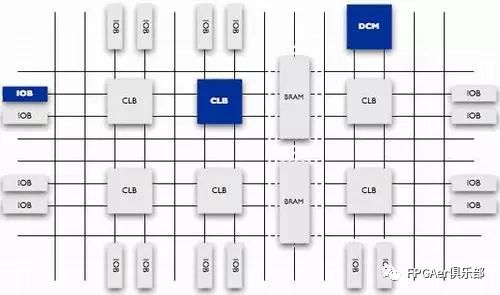
At present, mainstream FPGAs are still based on look-up table technology, which has far exceeded the basic performance of previous versions, and integrates hard core (ASIC-type) modules with common functions (such as RAM, clock management, and DSP). As shown in Figure 1-1 (Note: Figure 1-1 is only a schematic diagram, in fact, each series of FPGA has its corresponding internal structure), FPGA chip is mainly completed by 6 parts, namely: programmable input and output unit , Basic programmable logic unit, complete clock management, embedded block RAM, abundant wiring resources, embedded low-level functional units and embedded dedicated hardware modules.

Figure 1-1 The internal structure of the FPGA chip
The functions of each module are as follows:
1. Programmable input output unit (IOB)

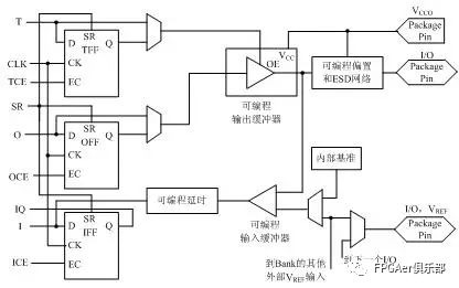
Figure 1-2 Schematic diagram of the internal structure of a typical IOB
The external input signal can be input to the inside of the FPGA through the storage unit of the IOB module, or directly input to the inside of the FPGA. When the external input signal is input into the FPGA through the storage unit of the IOB module, the hold time (Hold Time) requirement can be reduced, and it is usually 0 by default.
In order to facilitate management and adapt to a variety of electrical standards, FPGA IOB is divided into several banks (bank), the interface standard of each bank is determined by its interface voltage VCCO, a bank can only have one type of VCCO, but different banks of VCCO can be different. Only ports with the same electrical standard can be connected together, and the same VCCO voltage is the basic condition of the interface standard.
2. Configurable logic block (CLB)
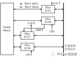
CLB is the basic logic unit in FPGA. The actual number and characteristics of CLBs will vary from device to device, but each CLB contains a configurable switch matrix, which consists of 4 or 6 inputs, some selection circuits (multiplexers, etc.) and flip-flops composition. The switch matrix is ​​highly flexible and can be configured to handle combinatorial logic, shift registers, or RAM. In Xilinx's FPGA devices, CLB is composed of multiple (generally 4 or 2) identical Slices and additional logic, as shown in Figure 1-3. Each CLB module can not only be used to implement combinational logic and sequential logic, but also can be configured as distributed RAM and distributed ROM.

Figure 1-3 Schematic diagram of a typical CLB structure
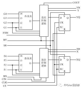
Slice is the basic logic unit defined by Xilinx. Its internal structure is shown in Figure 1-4. A slice is composed of two 4-input functions, carry logic, arithmetic logic, storage logic, and function multiplexer. Arithmetic logic includes an exclusive OR gate (XORG) and a dedicated AND gate (MULTAND). An exclusive OR gate can enable a slice to implement a 2bit full addition operation. The dedicated AND gate is used to improve the efficiency of the multiplier; the carry logic consists of a dedicated carry signal It is composed of function multiplexer (MUXC) to realize fast arithmetic addition and subtraction operations; 4-input function generator is used to realize 4-input LUT, distributed RAM or 16-bit shift register (in the Slice of Virtex-5 series chips) The two input functions are 6 inputs, which can realize 6-input LUT or 64-bit shift register); carry logic includes two fast carry chains to improve the processing speed of the CLB module.

Figure 1-4 Schematic diagram of a typical 4-input slice structure
3. Digital Clock Management Module (DCM)
Most FPGAs in the industry provide digital clock management (all Xilinx FPGAs have this feature). Xilinx introduced the most advanced FPGA to provide digital clock management and phase loop lock. The phase loop lock can provide accurate clock synthesis, and can reduce jitter, and realize the filtering function.
4. Embedded Block RAM (BRAM)
Most FPGAs have built-in block RAM, which greatly expands the scope and flexibility of FPGA applications. Block RAM can be configured as common storage structures such as single-port RAM, dual-port RAM, content address memory (CAM), and FIFO. RAM and FIFO are relatively popular concepts, so I won't repeat them here. The CAM memory has a comparison logic in each storage unit inside. The data written in the CAM will be compared with each internal data, and the address of all the data that is the same as the port data will be returned, so in the routing address There are a wide range of applications in exchangers. In addition to block RAM, the LUT in the FPGA can also be flexibly configured into structures such as RAM, ROM, and FIFO. In practical applications, the amount of block RAM inside the chip is also an important factor in choosing a chip.
The capacity of a single block RAM is 18k bits, that is, the bit width is 18 bits and the depth is 1024. The bit width and depth can be changed as needed, but two principles must be met: First, the modified capacity (bit width depth) cannot be greater than 18k bits; secondly, the maximum bit width cannot exceed 36 bits. Of course, multiple blocks of RAM can be cascaded to form a larger RAM. At this time, it is only limited by the number of block RAMs in the chip, and is no longer restricted by the above two principles.
5. Rich wiring resources
The wiring resource connects all the units inside the FPGA, and the length and craft of the connection determine the driving capability and transmission speed of the signal on the connection. There are abundant wiring resources inside the FPGA chip, which are divided into four different categories according to the process, length, width, and distribution location. The first category is global routing resources, which are used for the internal global clock and global reset/set routing of the chip; the second category is long-line resources, which are used to complete the routing of high-speed signals between chip banks and the second global clock signal; third Type is short-line resources, used to complete the logic interconnection and wiring between basic logic units; the fourth type is distributed wiring resources, used for proprietary clock, reset and other control signal lines.
In practice, the designer does not need to directly select wiring resources. The place and route device can automatically select wiring resources to connect each module unit according to the topology and constraint conditions of the input logic netlist. Essentially, there is a close and direct relationship between the use of wiring resources and the result of the design.
6. Built-in functional unit on the bottom layer
Embedded function modules mainly refer to DLL (Delay Locked Loop), PLL (Phase Locked Loop), DSP and CPU and other soft processing cores (Soft Core). Nowadays, more and more abundant embedded functional units have made the single-chip FPGA a system-level design tool, enabling it to have the capability of software and hardware joint design, and gradually transition to the SOC platform.
DLL and PLL have similar functions, which can perform clock multiplication and division with high precision and low jitter, as well as duty cycle adjustment and shift equalization functions. The chip produced by Xilinx Company integrates DLL, the chip of Altera Company integrates PLL, and the new chip of Lattice Company integrates PLL and DLL at the same time. PLL and DLL can be easily managed and configured by tools generated by the IP core. The structure of the DLL is shown in Figure 1-5.

Figure 1-5 Schematic diagram of a typical DLL module
7. Embedded dedicated hard core
The embedded dedicated hard core is relative to the soft core embedded in the bottom layer. It refers to the hard core (Hard Core) with powerful FPGA processing capability, which is equivalent to an ASIC circuit. In order to improve FPGA performance, chip manufacturers have integrated some dedicated hard cores inside the chip. For example: In order to increase the multiplication speed of FPGA, mainstream FPGAs have integrated dedicated multipliers; in order to adapt to communication bus and interface standards, many high-end FPGAs have integrated serial and parallel transceivers (SERDES), which can reach tens of Gbps. Sending and receiving speed. Xilinx's high-end products not only integrate Power PC series CPUs, but also embed DSP Core modules. The corresponding system-level design tools are EDK and Platform Studio, and the concept of System on Chip (System on Chip) is proposed accordingly. Through PowerPC, Miroblaze, Picoblaze and other platforms, standard DSP processors and related applications can be developed to achieve the development goals of SOC.
1.2.3 The concepts of soft core, hard core and solid core
IP (Intelligent Property) core is the general name of integrated circuit cores with intellectual property cores. It is a repeatedly verified macro module with specific functions. It has nothing to do with the chip manufacturing process and can be transplanted to different semiconductor processes. At the SOC stage, IP core design has become an important task for ASIC circuit design companies and FPGA providers, and it is also a manifestation of its strength. For FPGA development software, the more abundant IP cores it provides, the more convenient the user's design and the higher its market occupancy rate. At present, the IP core has become the basic unit of system design and has been exchanged, transferred and sold as an independent design result.
In terms of the way in which IP cores are provided, they are usually divided into three categories: soft cores, hard cores, and solid cores. In terms of the cost to complete the IP core, the hard core is the most expensive; in terms of flexibility in use, the soft core has the highest reusability.
1. In the field of EDA design, soft core refers to the register transfer level (RTL) model before synthesis; in FPGA design, it refers to the hardware language description of the circuit, including logic description, netlist, and help files. The soft core only undergoes functional simulation and needs to be synthesized and placed and routed before it can be used. Its advantages are high flexibility, strong portability, and allow users to configure themselves; the disadvantage is that the predictability of the module is low, there is a possibility of error in the subsequent design, and there is a certain design risk. Soft core is the most widely used form of IP core.
2. In the field of EDA design, solid core refers to a netlist with plan information; specifically, it can be regarded as a soft core with layout plan in FPGA design, and is usually provided in a mixed form of RTL code and corresponding specific process netlist . Combine the RTL description with the specific standard cell library for comprehensive optimization design to form a gate-level netlist, which can then be used with a layout tool. Compared with soft core, the design flexibility of solid core is slightly worse, but the reliability is greatly improved. At present, solid core is also one of the mainstream forms of IP core.
3. In the field of EDA design, hard core refers to a verified design layout; specifically in FPGA design, it refers to a design with a fixed layout and process, and a front-end and back-end verified design, and designers cannot modify it. There are two reasons why it cannot be modified: first, the system design has strict requirements on the timing of each module, and it is not allowed to disturb the existing physical layout; second, the requirement to protect intellectual property rights, and designers are not allowed to make any changes to it. The non-modifiable characteristics of IP hard cores make it difficult to reuse, so they can only be used in certain specific applications and have a narrow range of use.
Antenk mini usb:The small USB socket found on digital cameras, external hard drives, USB hubs and other equipment. Mini USB is much smaller than USB Type A and B but twice as thick as Micro USB (see illustration below).
MINI USB, also known as Mini USB, is a USB interface standard. USB is the abbreviation of universal serial bus in English, which means "universal serial bus" in Chinese. It is a technology developed for data transmission between PC and digital devices. Standard USB, MINIUSB and microusb have become the most common USB interfaces. Compared with standard USB, MINIUSB is smaller and suitable for small electronic devices such as mobile devices.
Mini USB is divided into a type, B type and ab type. Minib type 5pin interface is the most common interface. Due to its excellent anti misplug performance and small size, it is gaining the favor of many manufacturers. This interface is widely used in card readers, MP3, digital cameras and mobile hard disks.
Mini USB a, B connectors and their contacts (not drawn to scale) Mini USB Connector contact function
1 VBUS (4.4–5.25 V)
2 D−
3 D+
4 ID
5 grounding
The ID foot is only used in OTG function. The Mini USB interface is divided into mini-a, B and ab interfaces. If your system is only used as a slave, then use the B interface. The system controller will judge the level of the ID pin and determine what kind of device is inserted. If it is Gaoping, it is the B connector. At this time, the system will do slave mode. If the ID is low, it will be a interface. Then the system will use HNP dialogue protocol to decide which is the master and which is the slave
OTG is the abbreviation of on the go, that is, OTG technology is to realize the data transmission between devices without host. It is mainly used in the connection between different devices or mobile devices for data exchange. For example, the digital camera is directly connected to the printer, and through OTG technology, the USB port between two devices is connected to print out the photos taken immediately; the data in the digital camera can also be sent to the mobile hard disk of USB interface through OTG, so there is no need to carry expensive memory card or carry a portable computer for field operation.
Except for pin 4, other interface functions of Mini USB are the same as those of standard USB. The fourth needle becomes the ID, which is connected to the fifth needle on the mini-a, and can be suspended in the mini-b or connected to the fifth needle.
Mini USB
ShenZhen Antenk Electronics Co,Ltd , https://www.antenkcon.com